What is a filter?
Filter circuits are used in a wide variety of applications. In the field of telecommunication, band-pass filters are used in the audio frequency range (0 kHz to 20 kHz) for modems and speech processing. High-frequency band-pass filters (several hundred MHz) are used for channel selection in telephone central offices. Data acquisition systems usually require anti-aliasing low-pass filters as well as low-pass noise filters in their preceding signal conditioning stages. System power supplies often use band-rejection filters to suppress the 60-Hz line frequency and high frequency transients.
In addition, there are filters that do not filter any frequencies of a complex input signal, but just add a linear phase shift to each frequency component, thus contributing to a constant time delay. These are called all-pass filters. At high frequencies (> 1 MHz), all of these filters usually consist of passive components such as inductors (L), resistors (R), and capacitors (C). They are then called LRC filters.
In the lower frequency range (1 Hz to 1 MHz), however, the inductor value becomes very large and the inductor itself gets quite bulky, making economical production difficult. In these cases, active filters become important. Active filters are circuits that use an operational amplifier (op amp) as the active device in combination with some resistors and capacitors to provide an LRC-like filter performance at low frequencies (Figure 16–1).

Figure 16–1. Second-Order Passive Low-Pass and Second-Order Active Low-Pass
This chapter covers active filters. It introduces the three main filter optimizations (Butterworth, Tschebyscheff, and Bessel), followed by five sections describing the most common active filter applications: low-pass, high-pass, band-pass, band-rejection, and all-pass filters. Rather than resembling just another filter book, the individual filter sections are written in a cookbook style, thus avoiding tedious mathematical derivations. Each section starts with the general transfer function of a filter, followed by the design equations to calculate the individual circuit components. The chapter closes with a section on practical design hints for single-supply filter designs.
Fundamentals of Low-Pass Filters
The most simple low-pass filter is the passive RC low-pass network shown in Figure 16–2.

Figure 16–2. First-Order Passive RC Low-Pass
Its transfer function is:

where the complex frequency variable, s = jω+σ , allows for any time variable signals. For pure sine waves, the damping constant, σ, becomes zero and s = jω . For a normalized presentation of the transfer function, s is referred to the filter’s corner frequency, or –3 dB frequency, ωC, and has these relationships:

With the corner frequency of the low-pass in Figure 16–2 being fC = 1/2πRC, s becomes s = sRC and the transfer function A(s) results in:
The magnitude of the gain response is:
For frequencies Ω >> 1, the rolloff is 20 dB/decade. For a steeper rolloff, n filter stages can be connected in series as shown in Figure 16–3. To avoid loading effects, op amps, operating as impedance converters, separate the individual filter stages.

Figure 16–3. Fourth-Order Passive RC Low-Pass with Decoupling Amplifiers
The resulting transfer function is:

In the case that all filters have the same cut-off frequency, fC, the coefficients become
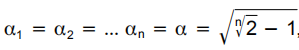
and fC of each partial filter is 1/α times higher than fC of the overall filter.
Figure 16–4 shows the results of a fourth-order RC low-pass filter. The rolloff of each partial filter (Curve 1) is –20 dB/decade, increasing the roll-off of the overall filter (Curve 2) to 80 dB/decade.
Note:
Filter response graphs plot gain versus the normalized frequency axis Ω (Ω = f/fC)
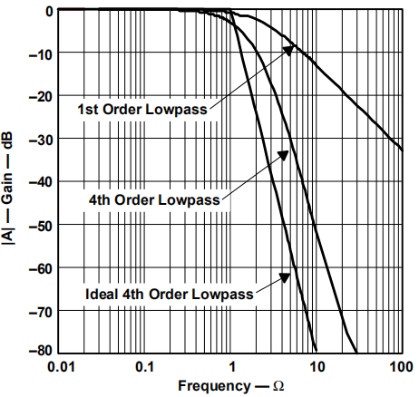
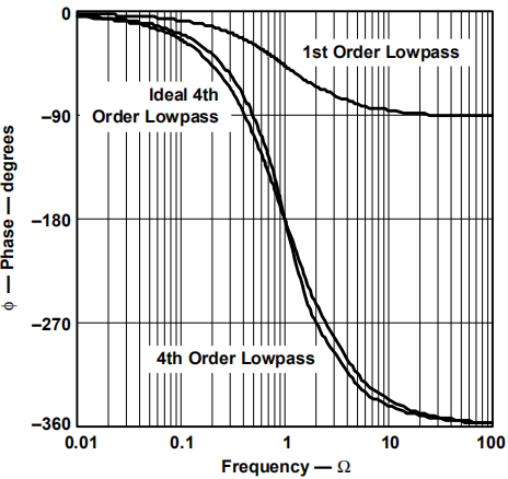
Note: Curve 1: 1st-order partial low-pass filter, Curve 2: 4th-order overall low-pass filter, Curve 3: Ideal 4th-order low-pass filter
Figure 16–4. Frequency and Phase Responses of a Fourth-Order Passive RC Low-Pass Filter
The corner frequency of the overall filter is reduced by a factor of α ≈ 2.3 times versus the –3 dB requency of partial filter stages.
In addition, Figure 16–4 shows the transfer function of an ideal fourth-order low-pass function (Curve 3).
In comparison to the ideal low-pass, the RC low-pass lacks in the following characteristics:
The passband gain varies long before the corner frequency, fC, thus amplifying the upper passband frequencies less than the lower passband.
The transition from the passband into the stopband is not sharp, but happens gradually, moving the actual 80-dB roll off by 1.5 octaves above fC.
The phase response is not linear, thus increasing the amount of signal distortion significantly.
The gain and phase response of a low-pass filter can be optimized to satisfy one of the following three criteria:
1) A maximum passband flatness,
2) An immediate passband-to-stopband transition,
3) A linear phase response.
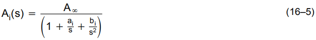
For that purpose, the transfer function must allow for complex poles and needs to be of the following type:

where A0 is the passband gain at dc, and ai and bi are the filter coefficients.
Since the denominator is a product of quadratic terms, the transfer function represents a series of cascaded second-order low-pass stages, with ai and bi being positive real coefficients. These coefficients define the complex pole locations for each second-order filter stage, thus determining the behavior of its transfer function.
The following three types of predetermined filter coefficients are available listed in table format in Section 16.9:
The Butterworth coefficients, optimizing the passband for maximum flatness
The Tschebyscheff coefficients, sharpening the transition from passband into the stopband
The Bessel coefficients, linearizing the phase response up to fC
The transfer function of a passive RC filter does not allow further optimization, due to the lack of complex poles. The only possibility to produce conjugate complex poles using passive components is the application of LRC filters. However, these filters are mainly used at high frequencies. In the lower frequency range (< 10 MHz) the inductor values become very large and the filter becomes uneconomical to manufacture. In these cases active filters are used.
Active filters are RC networks that include an active device, such as an operational amplifier (op amp).
Section 16.3 shows that the products of the RC values and the corner frequency must yield the predetermined filter coefficients ai and bi , to generate the desired transfer function.
The following paragraphs introduce the most commonly used filter optimizations.
1. Butterworth Low-Pass FIlters
The Butterworth low-pass filter provides maximum passband flatness. Therefore, a Butterworth low-pass is often used as anti-aliasing filter in data converter applications where precise signal levels are required across the entire passband.
Figure 16–5 plots the gain response of different orders of Butterworth low-pass filters versus the normalized frequency axis, Ω (Ω = f / fC); the higher the filter order, the longer the passband flatness.
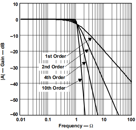
Figure 16–5. Amplitude Responses of Butterworth Low-Pass Filters
2. Tschebyscheff Low-Pass Filters
The Tschebyscheff low-pass filters provide an even higher gain rolloff above fC. However, as Figure 16–6 shows, the passband gain is not monotone, but contains ripples of constant magnitude instead. For a given filter order, the higher the passband ripples, the higher the filter’s rolloff.

Figure 16–6. Gain Responses of Tschebyscheff Low-Pass Filters
With increasing filter order, the influence of the ripple magnitude on the filter rolloff diminishes.
Each ripple accounts for one second-order filter stage. Filters with even order numbers generate ripples above the 0-dB line, while filters with odd order numbers create ripples below 0 dB.
Tschebyscheff filters are often used in filter banks, where the frequency content of a signal is of more importance than a constant amplification.
3. Bessel Low-Pass Filters
The Bessel low-pass filters have a linear phase response (Figure 16–7) over a wide frequency range, which results in a constant group delay (Figure 16–8) in that frequency range. Bessel low-pass filters, therefore, provide an optimum square-wave transmission behavior. However, the passband gain of a Bessel low-pass filter is not as flat as that of the Butterworth low-pass, and the transition from passband to stopband is by far not as sharp as that of a Tschebyscheff low-pass filter (Figure 16–9).
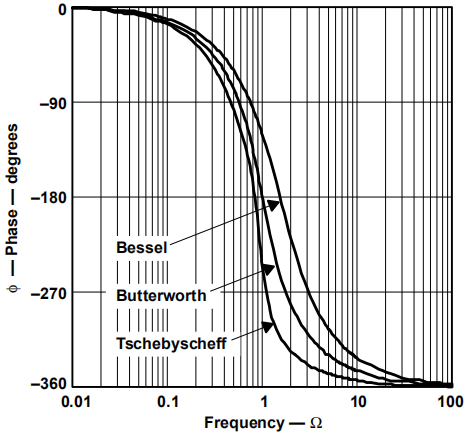
Figure 16–7. Comparison of Phase Responses of Fourth-Order Low-Pass Filters
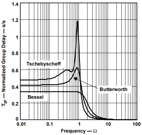
Figure 16–8. Comparison of Normalized Group Delay (Tgr) of Fourth-Order Low-Pass Filters
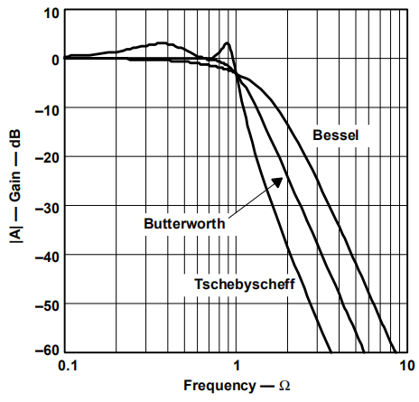
Figure 16–9. Comparison of Gain Responses of Fourth-Order Low-Pass Filters
4. Quality Factor Q
The quality factor Q is an equivalent design parameter to the filter order n. Instead of designing an nth order Tschebyscheff low-pass, the problem can be expressed as designing a Tschebyscheff low-pass filter with a certain Q.
For band-pass filters, Q is defined as the ratio of the mid frequency, fm, to the bandwidth at the two –3 dB points:

For low-pass and high-pass filters, Q represents the pole quality and is defined as:

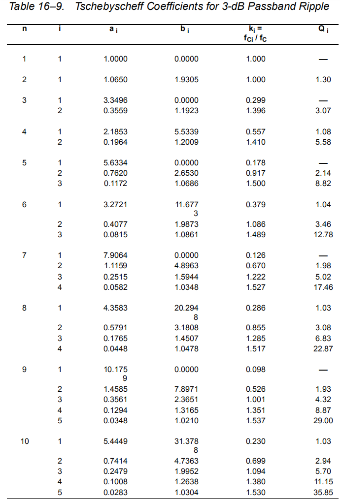
High Qs can be graphically presented as the distance between the 0-dB line and the peak point of the filter’s gain response. An example is given in Figure 16–10, which shows a tenth-order Tschebyscheff low-pass filter and its five partial filters with their individual Qs.
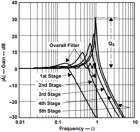
Figure 16–10. Graphical Presentation of Quality Factor Q on a Tenth-Order Tschebyscheff Low-Pass Filter with 3-dB Passband Ripple
The gain response of the fifth filter stage peaks at 31 dB, which is the logarithmic value of Q5:
Solving for the numerical value of Q5 yields:
which is within 1% of the theoretical value of Q = 35.85 given in Section 16.9, Table 16–9, last row. The graphical approximation is good for Q > 3. For lower Qs, the graphical values differ from the theoretical value significantly. However, only higher Qs are of concern, since the higher the Q is, the more a filter inclines to instability.
5. Summary
The general transfer function of a low-pass filter is :

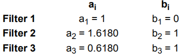
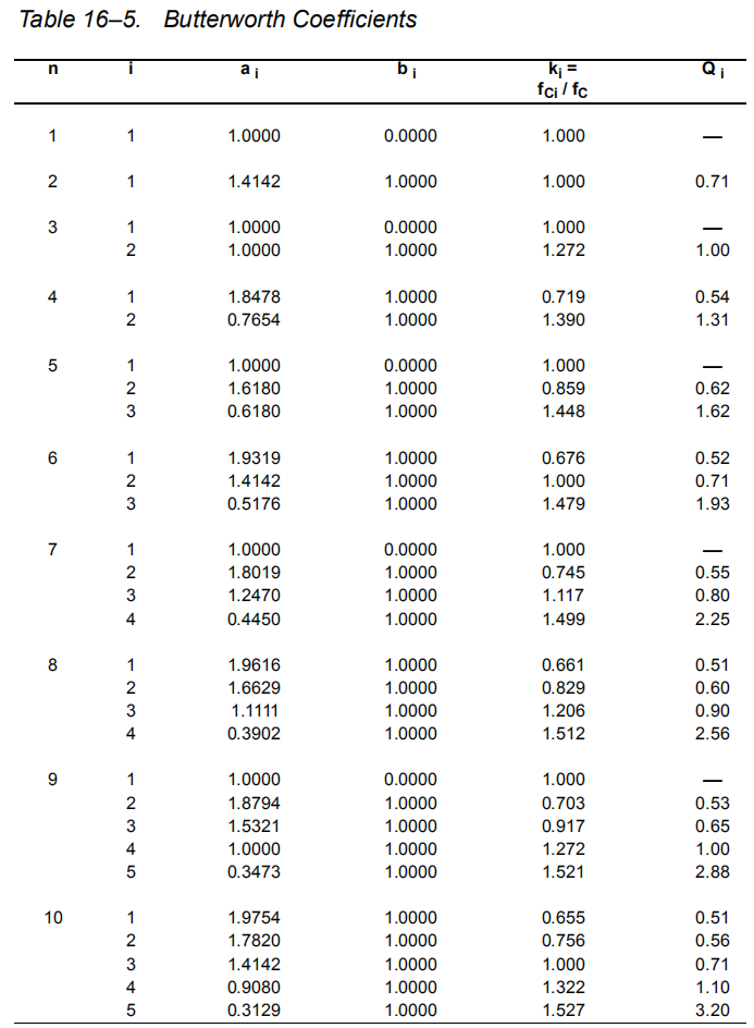
The filter coefficients ai and bi distinguish between Butterworth, Tschebyscheff, and Bessel filters. The coefficients for all three types of filters are tabulated down to the tenth order in Section 16.9, Tables 16–4 through 16–10.
The multiplication of the denominator terms with each other yields an nth order polynomial of S, with n being the filter order.
While n determines the gain rolloff above fC with n·20 dB/decade, ai and bi determine the gain behavior in the passband.
In addition, the ratio

is defined as the pole quality. The higher the Q value, the more a filter inclines to instability.
Low-Pass Filter Design
Equation 16–1 represents a cascade of second-order low-pass filters. The transfer function of a single stage is:

For a first-order filter, the coefficient b is always zero (b1=0), thus yielding:

The first-order and second-order filter stages are the building blocks for higher-order filters.
Often the filters operate at unity gain (A0=1) to lessen the stringent demands on the op amp’s open-loop gain.
Figure 16–11 shows the cascading of filter stages up to the sixth order. A filter with an even order number consists of second-order stages only, while filters with an odd order number include an additional first-order stage at the beginning.

Figure 16–11. Cascading Filter Stages for Higher-Order Filters
Figure 16–10 demonstrated that the higher the corner frequency of a partial filter, the higher its Q. Therefore, to avoid the saturation of the individual stages, the filters need to be placed in the order of rising Q values. The Q values for each filter order are listed (in rising order) in Section 16–9, Tables 16–4 through 16–10.
1. First-Order Low-Pass Filter
Figures 16–12 and 16–13 show a first-order low-pass filter in the inverting and in the noninverting configuration.

Figure 16–12. First-Order Noninverting Low-Pass Filter
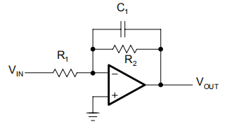
Figure 16–13. First-Order Inverting Low-Pass Filter
The transfer functions of the circuits are:

The negative sign indicates that the inverting amplifier generates a 180° phase shift from the filter input to the output.
The coefficient comparison between the two transfer functions and Equation 16–3 yields:

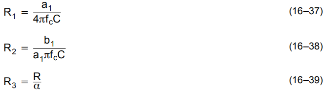
To dimension the circuit, specify the corner frequency (fC), the dc gain (A0), and capacitor C1, and then solve for resistors R1 and R2:

The coefficient a1 is taken from one of the coefficient tables, Tables 16–4 through 16–10.
Note, that all filter types are identical in their first order and a1 = 1. For higher filter orders, however, a1≠1 because the corner frequency of the first-order stage is different from the corner frequency of the overall filter.
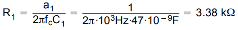
Example 16–1. First-Order Unity-Gain Low-Pass Filter
For a first-order unity-gain low-pass filter with fC = 1 kHz and C1 = 47 nF, R1 calculates to:
However, to design the first stage of a third-order unity-gain Bessel low-pass filter, assuming the same values for fC and C1, requires a different value for R1. In this case, obtain a1 for a third-order Bessel filter from Table 16–4 in Section 16.9 (Bessel coefficients) to calculate R1:
When operating at unity gain, the noninverting amplifier reduces to a voltage follower (Figure 16–14), thus inherently providing a superior gain accuracy. In the case of the inverting amplifier, the accuracy of the unity gain depends on the tolerance of the two resistors, R1 and R2.

Figure 16–14. First-Order Noninverting Low-Pass Filter with Unity Gain
2. Second-Order Low-Pass Filter
There are two topologies for a second-order low-pass filter, the Sallen-Key and the Multiple Feedback (MFB) topology.
2.1. Sallen-Key Topology
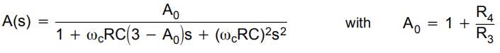
The general Sallen-Key topology in Figure 16–15 allows for separate gain setting via A0 = 1+R4/R3. However, the unity-gain topology in Figure 16–16 is usually applied in filter designs with high gain accuracy, unity gain, and low Qs (Q < 3).

Figure 16–15. General Sallen-Key Low-Pass Filter

Figure 16–16. Unity-Gain Sallen-Key Low-Pass Filter
The transfer function of the circuit in Figure 16–15 is:

For the unity-gain circuit in Figure 16–16 (A0=1), the transfer function simplifies to:

The coefficient comparison between this transfer function and Equation 16–2 yields:

Given C1 and C2, the resistor values for R1 and R2 are calculated through:
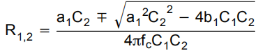
In order to obtain real values under the square root, C2 must satisfy the following condition:

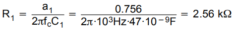
Example 16–2. Second-Order Unity-Gain Tschebyscheff Low-Pass Filter
The task is to design a second-order unity-gain Tschebyscheff low-pass filter with a corner frequency of fC = 3 kHz and a 3-dB passband ripple. From Table 16–9 (the Tschebyscheff coefficients for 3-dB ripple), obtain the coefficients a1 and b1 for a second-order filter with a1 = 1.0650 and b1 = 1.9305.
Specifying C1 as 22 nF yields in a C2 of:

Inserting a1 and b1 into the resistor equation for R1,2 results in:

with the final circuit shown in Figure 16–17.

Figure 16–17. Second-Order Unity-Gain Tschebyscheff Low-Pass with 3-dB Ripple
A special case of the general Sallen-Key topology is the application of equal resistor values and equal capacitor values: R1 = R2 = R and C1 = C2 = C.
The general transfer function changes to:
The coefficient comparison with Equation 16–2 yields:

Given C and solving for R and A0 results in:

Thus, A0 depends solely on the pole quality Q and vice versa; Q, and with it the filter type, is determined by the gain setting of A0:

The circuit in Figure 16–18 allows the filter type to be changed through the various resistor ratios R4/R3.

Figure 16–18. Adjustable Second-Order Low-Pass Filter
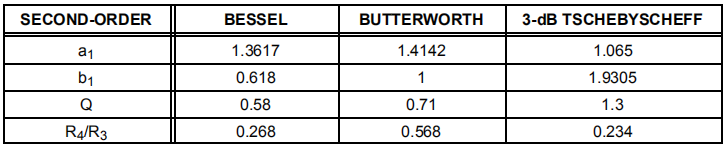
Table 16–1 lists the coefficients of a second-order filter for each filter type and gives the resistor ratios that adjust the Q.
Table 16–1. Second-Order FIlter Coefficients
2.2. Multiple Feedback Topology
The MFB topology is commonly used in filters that have high Qs and require a high gain.
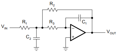
Figure 16–19. Second-Order MFB Low-Pass Filter
The transfer function of the circuit in Figure 16–19 is:

Through coefficient comparison with Equation 16–2 one obtains the relation:

Given C1 and C2, and solving for the resistors R1–R3:

In order to obtain real values for R2, C2 must satisfy the following condition:

3. Higher-Order Low-Pass Filters
Higher-order low-pass filters are required to sharpen a desired filter characteristic. For that purpose, first-order and second-order filter stages are connected in series, so that the product of the individual frequency responses results in the optimized frequency response of the overall filter.
In order to simplify the design of the partial filters, the coefficients ai and bi for each filter type are listed in the coefficient tables, with each table providing sets of coefficients for the first 10 filter orders.
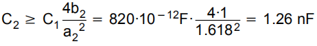
Example 16–3. Fifth-Order Filter
The task is to design a fifth-order unity-gain Butterworth low-pass filter with the corner frequency fC = 50 kHz.
First the coefficients for a fifth-order Butterworth filter:
Then dimension each partial filter by specifying the capacitor values and calculating the required resistor values.
First Filter
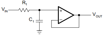
Figure 16–20. First-Order Unity-Gain Low-Pass
With C1 = 1nF,

The closest 1% value is 3.16 kΩ
Second Filter
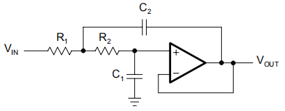
Figure 16–21. Second-Order Unity-Gain Sallen-Key Low-Pass Filter
With C1 = 820 pF,
The closest 5% value is 1.5 nF.
With C1 = 820 pF and C2 = 1.5 nF, calculate the values for R1 and R2 through:

and

and obtain,
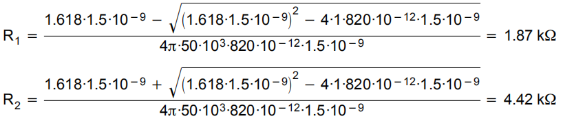
R1 and R2 are available 1% resistors.
Third Filter
The calculation of the third filter is identical to the calculation of the second filter, except that a2 and b2 are replaced by a3 and b3, thus resulting in different capacitor and resistor values.
Specify C1 as 330 pF, and obtain C2 with:

The closest 10% value is 4.7 nF.
With C1 = 330 pF and C2 = 4.7 nF, the values for R1 and R2 are:
R1 = 1.45 kΩ, with the closest 1% value being 1.47 kΩ
R2 = 4.51 kΩ, with the closest 1% value being 4.53 kΩ
Figure 16–22 shows the final filter circuit with its partial filter stages.
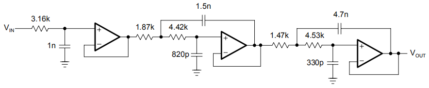
Figure 16–22. Fifth-Order Unity-Gain Butterworth Low-Pass Filter
High-Pass Filter Design
By replacing the resistors of a low-pass filter with capacitors, and its capacitors with resistors, a high-pass filter is created.
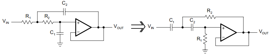
Figure 16–23. Low-Pass to High-Pass Transition Through Components Exchange
To plot the gain response of a high-pass filter, mirror the gain response of a low-pass filter at the corner frequency, Ω=1, thus replacing Ω with 1/Ω and S with 1/S in Equation 16–1.

Figure 16–24. Developing The Gain Response of a High-Pass Filter
The general transfer function of a high-pass filter is then:

with A∞ being the passband gain.
Since Equation 16–4 represents a cascade of second-order high-pass filters, the transfer function of a single stage is:
With b=0 for all first-order filters, the transfer function of a first-order filter simplifies to:
1. First-Order High-Pass Filter
Figure 16–25 and 16–26 show a first-order high-pass filter in the noninverting and the inverting configuration.
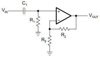
Figure 16–25. First-Order Noninverting High-Pass Filter

Figure 16–26. First-Order Inverting High-Pass Filter
The transfer functions of the circuits are:

The negative sign indicates that the inverting amplifier generates a 180° phase shift from the filter input to the output.
The coefficient comparison between the two transfer functions and Equation 16–6 provides two different passband gain factors:
while the term for the coefficient a1 is the same for both circuits:

To dimension the circuit, specify the corner frequency (fC), the dc gain (A∞), and capacitor (C1), and then solve for R1 and R2:

2. Second-Order High-Pass Filter
High-pass filters use the same two topologies as the low-pass filters: Sallen-Key and Multiple Feedback. The only difference is that the positions of the resistors and the capacitors have changed.
2.1. Sallen-Key Topology
The general Sallen-Key topology in Figure 16–27 allows for separate gain setting via A0 = 1+R4/R3.

Figure 16–27. General Sallen-Key High-Pass Filter
The transfer function of the circuit in Figure 16–27 is:

The unity-gain topology in Figure 16–28 is usually applied in low-Q filters with high gain accuracy.

Figure 16–28. Unity-Gain Sallen-Key High-Pass Filter
To simplify the circuit design, it is common to choose unity-gain (α = 1), and C1 = C2 = C. The transfer function of the circuit in Figure 16–28 then simplifies to:
The coefficient comparison between this transfer function and Equation 16–5 yields:

Given C, the resistor values for R1 and R2 are calculated through:

2.2. Multiple Feedback Topology
The MFB topology is commonly used in filters that have high Qs and require a high gain. To simplify the computation of the circuit, capacitors C1 and C3 assume the same value (C1 = C3 = C) as shown in Figure 16–29.
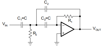
Figure 16–29. Second-Order MFB High-Pass Filter
The transfer function of the circuit in Figure 16–29 is:

Through coefficient comparison with Equation 16–5, obtain the following relations:

Given capacitors C and C2, and solving for resistors R1 and R2:
The passband gain (A∞) of a MFB high-pass filter can vary significantly due to the wide tolerances of the two capacitors C and C2. To keep the gain variation at a minimum, it is necessary to use capacitors with tight tolerance values.
3. Higher-Order High-Pass Filter
Likewise, as with the low-pass filters, higher-order high-pass filters are designed by cascading first-order and second-order filter stages. The filter coefficients are the same ones used for the low-pass filter design, and are listed in the coefficient tables (Tables 16–4 through 16–10 in Section 16.9).
Example 16–4. Third-Order High-Pass Filter with fC = 1 kHz
The task is to design a third-order unity-gain Bessel high-pass filter with the corner frequency fC = 1 kHz. Obtain the coefficients for a third-order Bessel filter:
and compute each partial filter by specifying the capacitor values and calculating the required resistor values.
First Filter
With C1 = 100 nF,
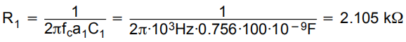
Closest 1% value is 2.1 kΩ.
Second Filter
With C = 100nF,

Closest 1% value is 3.16 kΩ.

Closest 1% value is 1.65 kΩ.
Figure 16–30 shows the final filter circuit.
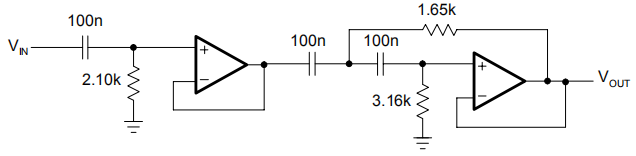
Figure 16–30. Third-Order Unity-Gain Bessel High-Pass
Band-Pass Filter Design
A high-pass response was generated by replacing the term S in the low pass transfer function with the transformation 1/S. Likewise, a band-pass characteristic is generated by replacing the S term with the transformation:
In this case, the passband characteristic of a low-pass filter is transformed into the upper passband half of a band-pass filter. The upper passband is then mirrored at the mid frequency, fm (Ω=1), into the lower passband half.

Figure 16–31. Low-Pass to Band-Pass Transition
The corner frequency of the low-pass filter transforms to the lower and upper –3 dB frequencies of the band-pass, Ω1 and Ω2. The difference between both frequencies is defined as the normalized bandwidth ∆Ω:
The normalized mid frequency, where Q = 1, is:
In analogy to the resonant circuits, the quality factor Q is defined as the ratio of the mid frequency (fm) to the bandwidth (B):

The simplest design of a band-pass filter is the connection of a high-pass filter and a lowpass filter in series, which is commonly done in wide-band filter applications. Thus, a first order high-pass and a first-order low-pass provide a second-order band-pass, while a second-order high-pass and a second-order low-pass result in a fourth-order band-pass response.
In comparison to wide-band filters, narrow-band filters of higher order consist of cascaded second-order band-pass filters that use the Sallen-Key or the Multiple Feedback (MFB) topology.
1. Second-Order Band-Pass Filter
To develop the frequency response of a second-order band-pass filter, apply the transformation in Equation 16–7 to a first-order low-pass transfer function:

Replacing s with

yields the general transfer function for a second-order band-pass filter:

When designing band-pass filters, the parameters of interest are the gain at the mid frequency (Am) and the quality factor (Q), which represents the selectivity of a band-pass filter.
Therefore, replace A0 with Am and ∆Ω with 1/Q (Equation 16–7) and obtain:

Figure 16–32 shows the normalized gain response of a second-order band-pass filter for different Qs.

Figure 16–32. Gain Response of a Second-Order Band-Pass Filter
The graph shows that the frequency response of second-order band-pass filters gets steeper with rising Q, thus making the filter more selective.
1.1. Sallen-Key Topology

Figure 16–33. Sallen-Key Band-Pass
The Sallen-Key band-pass circuit in Figure 16–33 has the following transfer function:

Through coefficient comparison with Equation 16–10, obtain the following equations:

The Sallen-Key circuit has the advantage that the quality factor (Q) can be varied via the inner gain (G) without modifying the mid frequency (fm). A drawback is, however, that Q and Am cannot be adjusted independently.
Care must be taken when G approaches the value of 3, because then Am becomes infinite and causes the circuit to oscillate.
To set the mid frequency of the band-pass, specify fm and C and then solve for R:

Because of the dependency between Q and Am, there are two options to solve for R2: either to set the gain at mid frequency:
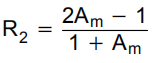
or to design for a specified Q:
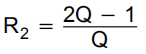
1.2. Multiple Feedback Topology
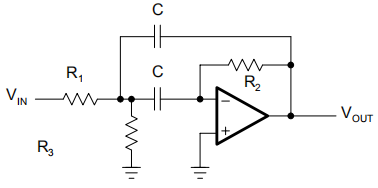
Figure 16–34. MFB Band-Pass
The MFB band-pass circuit in Figure 16–34 has the following transfer function:

The coefficient comparison with Equation 16–9, yields the following equations:

The MFB band-pass allows to adjust Q, Am, and fm independently. Bandwidth and gain factor do not depend on R3. Therefore, R3 can be used to modify the mid frequency without affecting bandwidth, B, or gain, Am. For low values of Q, the filter can work without R3, however, Q then depends on Am via:
Example 16–5. Second-Order MFB Band-Pass Filter with fm = 1 kHz
To design a second-order MFB band-pass filter with a mid frequency of fm = 1 kHz, a quality factor of Q = 10, and a gain of Am = –2, assume a capacitor value of C = 100 nF, and solve the previous equations for R1 through R3 in the following sequence:

2. Fourth-Order Band-Pass Filter (Staggered Tuning)
Figure 16–32 shows that the frequency response of second-order band-pass filters gets steeper with rising Q. However, there are band-pass applications that require a flat gain response close to the mid frequency as well as a sharp passband-to-stopband transition.
These tasks can be accomplished by higher-order band-pass filters. Of particular interest is the application of the low-pass to band-pass transformation onto a second-order low-pass filter, since it leads to a fourth-order band-pass filter.
Replacing the S term in Equation 16–2 with Equation 16–7 gives the general transfer function of a fourth-order band-pass:

Similar to the low-pass filters, the fourth-order transfer function is split into two second-order band-pass terms. Further mathematical modifications yield:

Equation 16–12 represents the connection of two second-order band-pass filters in series, where
Ami is the gain at the mid frequency, fmi, of each partial filter
Qi is the pole quality of each filter
α and 1/α are the factors by which the mid frequencies of the individual filters, fm1 and fm2, derive from the mid frequency, fm, of the overall bandpass.
In a fourth-order band-pass filter with high Q, the mid frequencies of the two partial filters differ only slightly from the overall mid frequency. This method is called staggered tuning.
Factor α needs to be determined through successive approximation, using equation 16–13:

with a1 and b1 being the second-order low-pass coefficients of the desired filter type.
To simplify the filter design, Table 16–2 lists those coefficients, and provides the α values for three different quality factors, Q = 1, Q = 10, and Q = 100.
Table 16–2. Values of α For Different Filter Types and Different Qs

After α has been determined, all quantities of the partial filters can be calculated using the following equations:
The mid frequency of filter 1 is:

the mid frequency of filter 2 is:
with fm being the mid frequency of the overall forth-order band-pass filter.
The individual pole quality, Qi , is the same for both filters:

with Q being the quality factor of the overall filter.
The individual gain (Ami) at the partial mid frequencies, fm1 and fm2, is the same for both filters:
with Am being the gain at mid frequency, fm, of the overall filter.
Example 16–6. Fourth-Order Butterworth Band-Pass Filter
The task is to design a fourth-order Butterworth band-pass with the following parameters:
mid frequency, fm = 10 kHz
bandwidth, B = 1000 Hz
and gain, Am = 1
From Table 16–2 the following values are obtained:
a1 = 1.4142
b1 = 1
α = 1.036
In accordance with Equations 16–14 and 16–15, the mid frequencies for the partial filters are:
The overall Q is defined as Q = fm/B , and for this example results in Q = 10.
Using Equation 16–16, the Qi of both filters is:

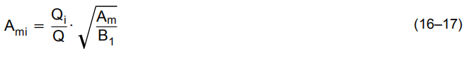
With Equation 16–17, the passband gain of the partial filters at fm1 and fm2 calculates to:
The Equations 16–16 and 16–17 show that Qi and Ami of the partial filters need to be independently adjusted. The only circuit that accomplishes this task is the MFB band-pass filter.
To design the individual second-order band-pass filters, specify C = 10 nF, and insert the previously determined quantities for the partial filters into the resistor equations of the MFB band-pass filter. The resistor values for both partial filters are calculated below.

Figure 16–35 compares the gain response of a fourth-order Butterworth band-pass filter with Q = 1 and its partial filters to the fourth-order gain of Example 16–4 with Q = 10.

Figure 16–35. Gain Responses of a Fourth-Order Butterworth Band-Pass and its Partial Filters
Band-Rejection Filter Design
A band-rejection filter is used to suppress a certain frequency rather than a range of frequencies.
Two of the most popular band-rejection filters are the active twin-T and the active Wien Robinson circuit, both of which are second-order filters.
To generate the transfer function of a second-order band-rejection filter, replace the S term of a first-order low-pass response with the transformation in 16–18:
which gives:

Thus the passband characteristic of the low-pass filter is transformed into the lower passband of the band-rejection filter. The lower passband is then mirrored at the mid frequency, fm (Ω=1), into the upper passband half (Figure 16–36).

Figure 16–36. Low-Pass to Band-Rejection Transition
The corner frequency of the low-pass transforms to the lower and upper –3-dB frequencies of the band-rejection filter Ω1 and Ω2. The difference between both frequencies is the normalized bandwidth ∆Ω:
Identical to the selectivity of a band-pass filter, the quality of the filter rejection is defined as:
Therefore, replacing ∆Ω in Equation 16–19 with 1/Q yields:

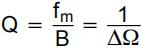
1. Active Twin-T Filter
The original twin-T filter, shown in Figure 16–37, is a passive RC-network with a quality factor of Q = 0.25. To increase Q, the passive filter is implemented into the feedback loop of an amplifier, thus turning into an active band-rejection filter, shown in Figure 16–38.

Figure 16–37. Passive Twin-T Filter
Figure 16–38. Active Twin-T Filter
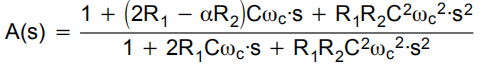
The transfer function of the active twin-T filter is:

Comparing the variables of Equation 16–21 with Equation 16–20 provides the equations that determine the filter parameters:

The twin-T circuit has the advantage that the quality factor (Q) can be varied via the inner gain (G) without modifying the mid frequency (fm). However, Q and Am cannot be adjusted independently.
To set the mid frequency of the band-pass, specify fm and C, and then solve for R:
Because of the dependency between Q and Am, there are two options to solve for R2: either to set the gain at mid frequency:
or to design for a specific Q:
2. Active Wien-Robinson Filter
The Wien-Robinson bridge in Figure 16–39 is a passive band-rejection filter with differential output. The output voltage is the difference between the potential of a constant voltage divider and the output of a band-pass filter. Its Q-factor is close to that of the twin-T circuit. To achieve higher values of Q, the filter is connected into the feedback loop of an amplifier.

Figure 16–39. Passive Wien-Robinson Bridge

Figure 16–40. Active Wien-Robinson Filter
The active Wien-Robinson filter in Figure 16–40 has the transfer function:
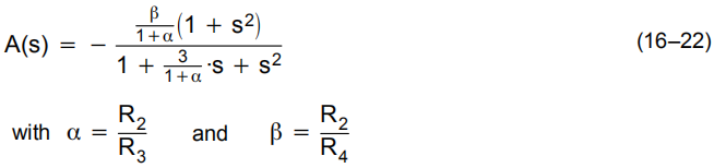
Comparing the variables of Equation 16–22 with Equation 16–20 provides the equations that determine the filter parameters:
To calculate the individual component values, establish the following design procedure:
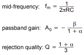
1) Define fm and C and calculate R with:
2) Specify Q and determine α via:
3) Specify A0 and determine β via:
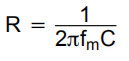
4) Define R2 and calculate R3 and R4 with:

and
In comparison to the twin-T circuit, the Wien-Robinson filter allows modification of the passband gain, A0, without affecting the quality factor, Q.
If fm is not completely suppressed due to component tolerances of R and C, a fine-tuning of the resistor 2R2 is required.
Figure 16–41 shows a comparison between the filter response of a passive band-rejection filter with Q = 0.25, and an active second-order filter with Q = 1, and Q = 10.
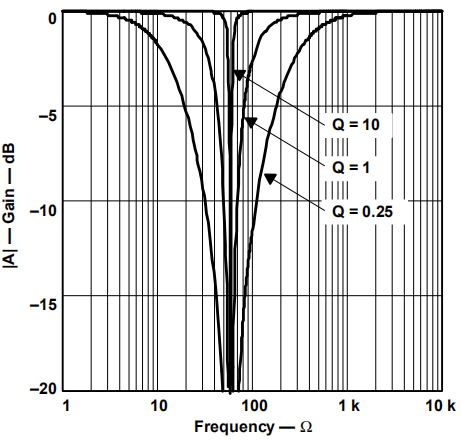
Figure 16–41. Comparison of Q Between Passive and Active Band-Rejection Filters
All-Pass Filter Design
In comparison to the previously discussed filters, an all-pass filter has a constant gain across the entire frequency range, and a phase response that changes linearly with frequency.
Because of these properties, all-pass filters are used in phase compensation and signal delay circuits.
Similar to the low-pass filters, all-pass circuits of higher order consist of cascaded first-order and second-order all-pass stages. To develop the all-pass transfer function from a low-pass response, replace A0 with the conjugate complex denominator.
The general transfer function of an allpass is then:

with ai and bi being the coefficients of a partial filter.
Expressing Equation 16–23 in magnitude and phase yields:

This gives a constant gain of 1, and a phase shift,φ, of:

To transmit a signal with minimum phase distortion, the all-pass filter must have a constant group delay across the specified frequency band. The group delay is the time by which the all-pass filter delays each frequency within that band.
The frequency at which the group delay drops to 1 / √2 –times its initial value is the corner frequency, fC.
The group delay is defined through:

To present the group delay in normalized form, refer tgr to the period of the corner frequency, TC, of the all-pass circuit:

Substituting tgr through Equation 16–26 gives:

Inserting the ϕ term in Equation 16–25 into Equation 16–28 and completing the derivation, results in:

Setting Ω = 0 in Equation 16–29 gives the group delay for the low frequencies, 0 < Ω < 1, which is:

In addition, Figure 16–42 shows the group delay response versus the frequency for the first ten orders of all-pass filters.

Figure 16–42. Frequency Response of the Group Delay for the First 10 Filter Orders
1. First-Order All-Pass Filter
Figure 16–43 shows a first-order all-pass filter with a gain of +1 at low frequencies and a gain of –1 at high frequencies. Therefore, the magnitude of the gain is 1, while the phase changes from 0° to –180°.

Figure 16–43. First-Order All-Pass
The transfer function of the circuit above is:

The coefficient comparison with Equation 16–23 (b1=1), results in:
To design a first-order all-pass, specify fC and C and then solve for R:

Inserting Equation 16–31 into 16–30 and substituting ωC with Equation 16–27 provides the maximum group delay of a first-order all-pass filter:
2. Second-Order All-Pass Filter
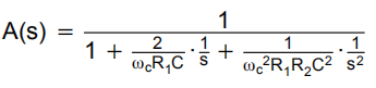
Figure 16–44 shows that one possible design for a second-order all-pass filter is to subtract the output voltage of a second-order band-pass filter from its input voltage.

Figure 16–44. Second-Order All-Pass Filter
The transfer function of the circuit in Figure 16–44 is:
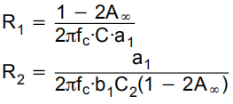
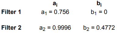
The coefficient comparison with Equation 16–23 yields:

To design the circuit, specify fC, C, and R, and then solve for the resistor values:
Inserting Equation 16–34 into Equation16–30 and substituting ωC with Equation 16–27 gives the maximum group delay of a second-order all-pass filter:
3. Higher-Order All-Pass Filter
Higher-order all-pass filters consist of cascaded first-order and second-order filter stages.
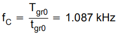
Example 16–7. 2-ms Delay All-Pass Filter
A signal with the frequency spectrum, 0 < f < 1 kHz, needs to be delayed by 2 ms. To keep the phase distortions at a minimum, the corner frequency of the all-pass filter must be fC ≥ 1 kHz.
Equation 16–27 determines the normalized group delay for frequencies below 1 kHz:

Figure 16–42 confirms that a seventh-order all-pass is needed to accomplish the desired delay. The exact value, however, is Tgr0 = 2.1737. To set the group delay to precisely 2 ms, solve Equation 16–27 for fC and obtain the corner frequency:
To complete the design, look up the filter coefficients for a seventh-order all-pass filter, specify C, and calculate the resistor values for each partial filter. Cascading the first-order all-pass with the three second-order stages results in the desired seventh-order all-pass filter.
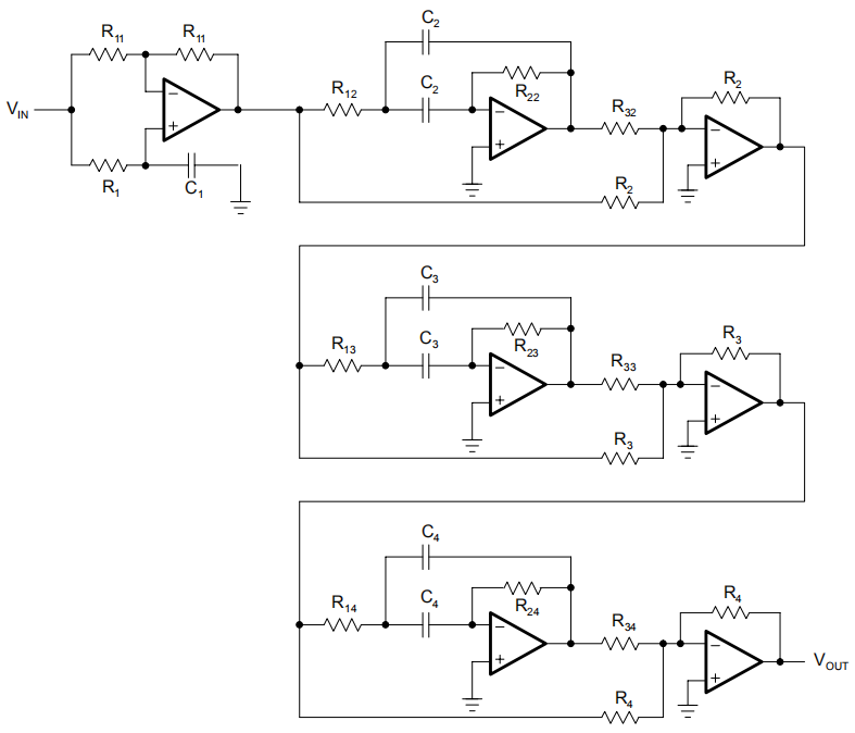
Figure 16–45. Seventh-Order All-Pass Filter
Practical Design Hints
introduces dc-biasing techniques for filter designs in single-supply applications, which are usually not required when operating with dual supplies. It also provides recommendations on selecting the type and value range of capacitors and resistors as well as the decision criteria for choosing the correct op amp.
1. Filter Circuit Biasing
The filter diagrams in this chapter are drawn for dual supply applications. The op amp operates from a positive and a negative supply, while the input and the output voltage are referenced to ground (Figure 16–46).
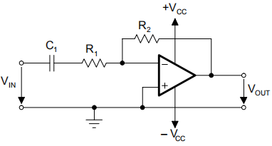
Figure 16–46. Dual-Supply Filter Circuit
For the single supply circuit in Figure 16–47, the lowest supply voltage is ground. For a symmetrical output signal, the potential of the noninverting input is level-shifted to midrail.

Figure 16–47. Single-Supply Filter Circuit
The coupling capacitor, CIN in Figure 16–47, ac-couples the filter, blocking any unknown dc level in the signal source. The voltage divider, consisting of the two equal-bias resistors RB, divides the supply voltage to VMID and applies it to the inverting op amp input. For simple filter input structures, passive RC networks often provide a low-cost biasing solution. In the case of more complex input structures, such as the input of a second-order low-pass filter, the RC network can affect the filter characteristic. Then it is necessary to either include the biasing network into the filter calculations, or to insert an input buffer between biasing network and the actual filter circuit, as shown in Figure 16–48.

Figure 16–48. Biasing a Sallen-Key Low-Pass
CIN ac-couples the filter, blocking any dc level in the signal source. VMID is derived from VCC via the voltage divider. The op amp operates as a voltage follower and as an impedance converter. VMID is applied via the dc path, R1 and R2, to the noninverting input of the filter amplifier.
Note that the parallel circuit of the resistors, RB , together with CIN create a high-pass filter. To avoid any effect on the low-pass characteristic, the corner frequency of the input high pass must be low versus the corner frequency of the actual low-pass.
The use of an input buffer causes no loading effects on the low-pass filter, thus keeping the filter calculation simple. In the case of a higher-order filter, all following filter stages receive their bias level from the preceding filter amplifier. Figure 16–49 shows the biasing of an multiple feedback (MFB) low-pass filter.

Figure 16–49. Biasing a Second-Order MFB Low-Pass Filter
The input buffer decouples the filter from the signal source. The filter itself is biased via the noninverting amplifier input. For that purpose, the bias voltage is taken from the output of a VMID generator with low output impedance. The op amp operates as a difference amplifier and subtracts the bias voltage of the input buffer from the bias voltage of the VMID generator, thus yielding a dc potential of VMID at zero input signal.
A low-cost alternative is to remove the op amp and to use a passive biasing network instead. However, to keep loading effects at a minimum, the values for RB must be significantly higher than without the op amp. The biasing of a Sallen-Key and an MFB high-pass filter is shown in Figure 16–50.
The input capacitors of high-pass filters already provide the ac-coupling between filter and signal source. Both circuits use the VMID generator from Figure 16–50 for biasing. While the MFB circuit is biased at the noninverting amplifier input, the Sallen-Key high-pass is biased via the only dc path available, which is R1. In the ac circuit, the input signals travel via the low output impedance of the op amp to ground.

Figure 16–50. Biasing a Sallen-Key and an MFB High-Pass Filter
2. Capacitor Selection
The tolerance of the selected capacitors and resistors depends on the filter sensitivity and on the filter performance.
Sensitivity is the measure of the vulnerability of a filter’s performance to changes in component values. The important filter parameters to consider are the corner frequency, fC, and Q.
For example, when Q changes by ± 2% due to a ± 5% change in the capacitance value, then the sensitivity of Q to capacity changes is expressed as:

The following sensitivity approximations apply to second-order Sallen-Key and MFB filters:
Although 0.5 %/% is a small difference from the ideal parameter, in the case of higher-order filters, the combination of small Q and fC differences in each partial filter can significantly modify the overall filter response from its intended characteristic.
Figures 16.51 and 16.52 show how an intended eighth-order Butterworth low-pass can turn into a low-pass with Tschebyscheff characteristic mainly due to capacitance changes from the partial filters.
Figure 16–51 shows the differences between the ideal and the actual frequency responses of the four partial filters. The overall filter responses are shown in Figure 16–52.
The difference between ideal and real response peaks with 0.35 dB at approximately 30 kHz, which is equivalent to an enormous 4.1% gain error can be seen.
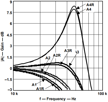
Figure 16–51. Differences in Q and fC in the Partial Filters of an Eighth-Order Butterworth Low-Pass Filter

Figure 16–52. Modification of the Intended Butterworth Response to a Tschebyscheff-Type Characteristic
If this filter is intended for a data acquisition application, it could be used at best in a 4-bit system. In comparison, if the maximum full-scale error of a 12-bit system is given with LSB, then maximum pass-band deviation would be – 0.001 dB, or 0.012%.
To minimize the variations of fC and Q, NPO (COG) ceramic capacitors are recommended for high-performance filters. These capacitors hold their nominal value over a wide temperature and voltage range. The various temperature characteristics of ceramic capacitors are identified by a three-symbol code such as: COG, X7R, Z5U, and Y5V.
COG-type ceramic capacitors are the most precise. Their nominal values range from 0.5 pF to approximately 47 nF with initial tolerances from ± 0.25 pF for smaller values and up to ±1% for higher values. Their capacitance drift over temperature is typically 30ppm/°C.
X7R-type ceramic capacitors range from 100 pF to 2.2 µF with an initial tolerance of +1% and a capacitance drift over temperature of ±15%. For higher values, tantalum electrolytic capacitors should be used.
Other precision capacitors are silver mica, metallized polycarbonate, and for high temperatures, polypropylene or polystyrene. Since capacitor values are not as finely subdivided as resistor values, the capacitor values should be defined prior to selecting resistors. If precision capacitors are not available to provide an accurate filter response, then it is necessary to measure the individual capacitor values, and to calculate the resistors accordingly.
For high performance filters, 0.1% resistors are recommended.
3. Component Values
Resistor values should stay within the range of 1 kΩ to 100 kΩ. The lower limit avoids excessive current draw from the op amp output, which is particularly important for single supply op amps in power-sensitive applications. Those amplifiers have typical output currents of between 1 mA and 5 mA. At a supply voltage of 5 V, this current translates to a minimum of 1 kΩ.
The upper limit of 100 kΩ is to avoid excessive resistor noise. Capacitor values can range from 1 nF to several µF. The lower limit avoids coming too close to parasitic capacitances. If the common-mode input capacitance of the op amp, used in a Sallen-Key filter section, is close to 0.25% of C1, (C1 / 400), it must be considered for accurate filter response. The MFB topology, in comparison, does not require input-capacitance compensation.
4. Op Amp Selection
The most important op amp parameter for proper filter functionality is the unity-gain bandwidth. In general, the open-loop gain (AOL) should be 100 times (40 dB above) the peak gain (Q) of a filter section to allow a maximum gain error of 1%.
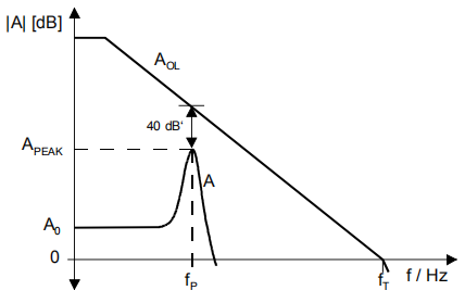
Figure 16–53. Open-Loop Gain (AOL) and Filter Response (A)
The following equations are good rules of thumb to determine the necessary unity-gain bandwidth of an op amp for an individual filter section.
1) First-order filter:
2) Second-order filter (Q < 1):

3) Second-order filter (Q > 1):

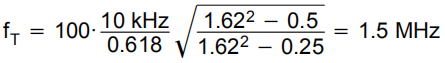
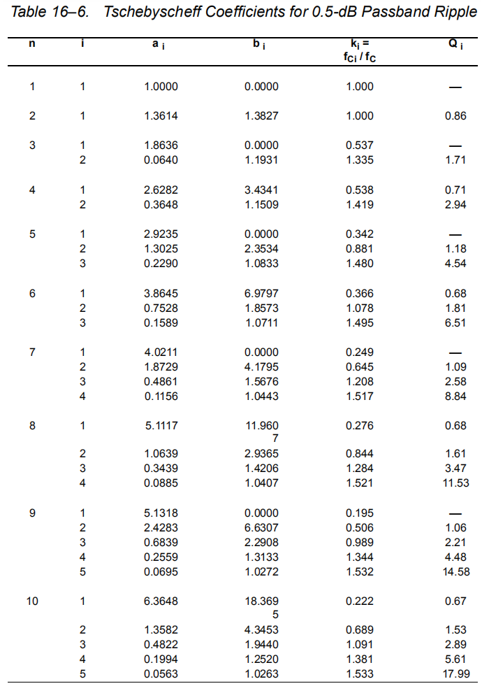
For example, a fifth-order, 10-kHz, Tschebyscheff low-pass filter with 3-dB passband ripple and a dc gain of A0 = 2 has its worst case Q in the third filter section. With Q3 = 8.82 and a3 = 0.1172, the op amp needs to have a unity-gain bandwidth of:

In comparison, a fifth-order unity-gain, 10-kHz, Butterworth low-pass filter has a worst case Q of Q3 = 1.62; a3 = 0.618. Due to the lower Q value, fT is also lower and calculates to only:
Besides good dc performance, low noise, and low signal distortion, another important parameter that determines the speed of an op amp is the slew rate (SR). For adequate full power response, the slew rate must be greater than:
For example, a single-supply, 100-kHz filter with 5 VPP output requires a slew rate of at least:
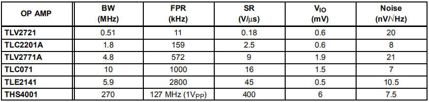
Texas Instruments offers a wide range of op amps for high-performance filters in single supply applications. Table 16–3 provides a selection of single-supply amplifiers sorted in order of rising slew rate.
Table 16–3. Single-Supply Op Amp Selection Guide (TA = 25°C, VCC = 5 V)
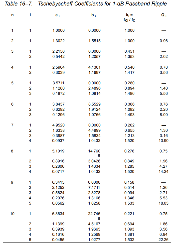
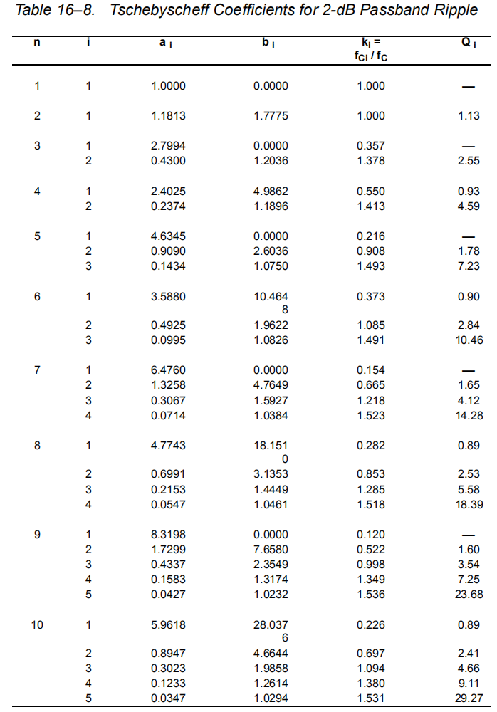
Filter Coefficient Tables
The following tables contain the coefficients for the three filter types, Bessel, Butterworth and Tschebyscheff. The Tschebyscheff tables (Table 16–9) are split into categories for the following passband ripples: 0.5 dB, 1 dB, 2 dB, and 3 dB.
The table headers consist of the following quantities:
n is the filter order
i is the number of the partial filter.
ai , bi are the filter coefficients.
ki is the ratio of the corner frequency of a partial filter, fCi , to the corner frequency of the overall filter, fC. This ratio is used to determine the unity-gain bandwidth of the op amp, as well as to simplify the test of a filter design by measuring fCi and comparing it to fC.
Qi is the quality factor of the partial filter.
fi / fC this ratio is used for test purposes of the allpass filters, where fi is the frequency, at which the phase is 180° for a second-order filter, respectively 90° for a first-order all-pass.
Tgr0 is the normalized group delay of the overall all-pass filter.


No comments:
Post a Comment