Introduction to Single-Supply Circuit Collection
Portable and single-supply electronic equipment is becoming more popular each day. The demand for single-supply op amp circuits increases with the demand for portable electronic equipment because most portable systems have one battery. Split- or dual-supply op amp circuit design is straightforward because op amp inputs and outputs are referenced to the normally grounded center tap of the supplies. In the majority of split-supply applications, signal sources driving the op amp inputs are referenced to ground, thus with one input of the op amp referenced to ground, as shown in Figure A–1, there is no need to consider input common-mode voltage problems.


Figure A–1. Split-Supply Op Amp Circuit
When the signal source is not referenced to ground (see Figure A–2 and Equation A–1B), the voltage difference between ground and the reference voltage shows up amplified in the output voltage. Sometimes this situation is OK, but other times the difference voltage must be stripped out of the output voltage.


Figure A–2. Split-Supply Op Amp Circuit With Reference Voltage Input
An input bias voltage is used to eliminate the difference voltage when it must not appear in the output voltage (see Figure A–3 and Equation A–1C). The voltage, VREF, is in both input circuits, hence it is named a common-mode voltage. Voltage-feedback op amps, like those used in this document, reject common-mode voltages because their input circuit is constructed with a differential amplifier (chosen because it has natural common-mode voltage rejection capabilities).


Figure A–3. Split-Supply Op Amp Circuit With Common-Mode Voltage
When signal sources are referenced to ground, single-supply op amp circuits always have a large input common-mode voltage. Figure A–4 shows a single-supply op amp circuit that has its input voltage referenced to ground. The input voltage is not referenced to the midpoint of the supplies like it would be in a split-supply application, rather it is referenced to the lower power supply rail. This circuit malfunctions when the input voltage is positive because the output voltage would have to go negative — hard to do with a positive supply. It operates marginally with small negative input voltages because most op amps do not function well when the inputs are connected to the supply rails.

Figure A–4. Single-Supply Op Amp Circuit
The constant requirement to account for inputs connected to ground or other reference voltages makes it difficult to design single-supply op amp circuits. This appendix presents a collection of single-supply op amp circuits, including their description and transfer equation. Those without a good working knowledge of op amp equations should reference the Understanding Basic Analog series of application notes available from Texas Instruments. Application note SLAA068, Understanding Basic Analog — Ideal Op Amps develops the ideal op amp equations. Circuit equations in this appendix are written with the ideal op amp assumptions as specified in Understanding Basic Analog — Ideal Op Amps.
The assumptions appear in Table A–1 for easy reference.
Table A–1. Ideal Op Amp Assumptions

Detailed information about designing single-supply op amp circuits appears in application note SLOA030, Single-Supply Op Amp Design Techniques. Unless otherwise specified, all op amp circuits shown here are single-supply circuits. The single supply may be wired with the negative or positive lead connected to ground, but as long as the supply polarity is correct, the wiring does not affect circuit operation.
Boundary Conditions
All op amps are constrained to output voltage swings less than or equal to their power supply. Use of a single supply limits the output voltage to the range of the supply voltage. For example, when the supply voltage VCC equals +10 V, the output voltage is limited to the range 0 ≤ VOUT ≤ 10. This limitation precludes negative output voltages when the circuit has a positive supply voltage, but it does not preclude negative input voltages. As long as the voltage on the op amp input leads does not become negative, the circuit can handle negative voltages applied to the input resistors.
Beware of working with negative (positive) input voltages when the op amp is powered from a positive (negative) supply because op amp inputs are highly susceptible to reverse-voltage breakdown. Also, ensure that no start-up condition reverse biases the op amp inputs when the input and supply voltage are opposite polarity. It may be advisable to protect the op amp inputs with a diode (Schottky or germanium) connected anode to ground and cathode to the op amp input.
Amplifiers
Many types of amplifiers can be created using op amps. This section consists of a selection of some basic, single-supply op amp circuits that are available to the designer during the concept stage of a design. The circuit configuration and correct single-supply dc biasing techniques are presented for the following cases: inverting, noninverting, differential, T-network, buffer and ac-coupled amplifiers.
1. Inverting Op Amp with Noninverting Positive Reference
The ideal transfer equation is given in Equation A–1.

The transfer equation for this circuit (Figure A–5) takes the form of Y = –mX + b. The transfer function slope is negative, and the dc intercept is positive. RF and RG are contained in both halves of the equation, thus it is hard to obtain the desired slope and dc intercept without modifying VREF. This is the minimum component count configuration for this transfer function. When the reference voltage is 0, the input voltage is constrained to negative voltages because positive input voltages would cause the output voltage to saturate at ground.

Figure A–5. Inverting Op Amp with Noninverting Positive Reference
2. Inverting Op Amp with Inverting Negative Reference
The transfer equation takes the form of Y = –mX + b and is given in Equation A–2.

The transfer function slope is negative, and the dc intercept is positive (Figure A–6). RG1 and RG2 are contained in the equation, thus it is easy to obtain the desired slope and dc intercept by adjusting the value of both resistors. Because of the virtual ground at the inverting input, RG2 is the terminating impedance for VREF. When the reference voltage is 0, the input voltage is constrained to negative voltages because positive input voltages would cause the output voltage to saturate at ground.

Figure A–6. Inverting Op Amp with Inverting Negative Reference
3. Inverting Op Amp with Noninverting Negative Reference
The transfer equation takes the form of Y = –mX – b and is given in Equation A–3.

The transfer function slope is negative, and the dc intercept is negative. RF and RG are contained in both halves of the equation, thus it is hard to obtain the desired slope and dc intercept without modifying VREF. This is the minimum component count configuration for this transfer function. The slope and dc intercept terms in Equation A–3 are both negative, hence, unless the correct input voltage range is selected, the output voltage will saturate at ground. The negative input voltage must be limited to less than –400 mV because op amp inputs either break down or have protection circuits that forward bias when large negative voltages are applied to the inputs.

Figure A–7. Inverting Op Amp with Noninverting Negative Reference
4. Inverting Op Amp with Inverting Positive Reference
The transfer equation takes the form of Y = –mX – b and is given in Equation A–4.

The transfer function slope is negative, and the dc intercept is negative. RG1 and RG2 are contained in the equation, thus it is easy to obtain the desired slope and dc intercept by adjusting the value of both resistors. Because of the virtual ground at the inverting input, RG2 is the terminating impedance for VREF. The slope and dc intercept terms in Equation A–4 are both negative, hence, unless the correct input voltage range is selected, the output voltage will saturate.

Figure A–8. Inverting Op Amp with Inverting Positive Reference
5. Noninverting Op Amp with Inverting Positive Reference
The transfer equation takes the form of Y = mX – b and is given in Equation A–5.

The transfer function slope is positive, and the dc intercept is negative. This is the minimum component count configuration for this transfer function. The reference termination resistor is connected to a virtual ground, so RG is the load across VREF. RF and RG are contained in both halves of the equation, thus it is hard to obtain the desired slope and dc intercept without modifying VREF or placing an attenuator in series with VIN.
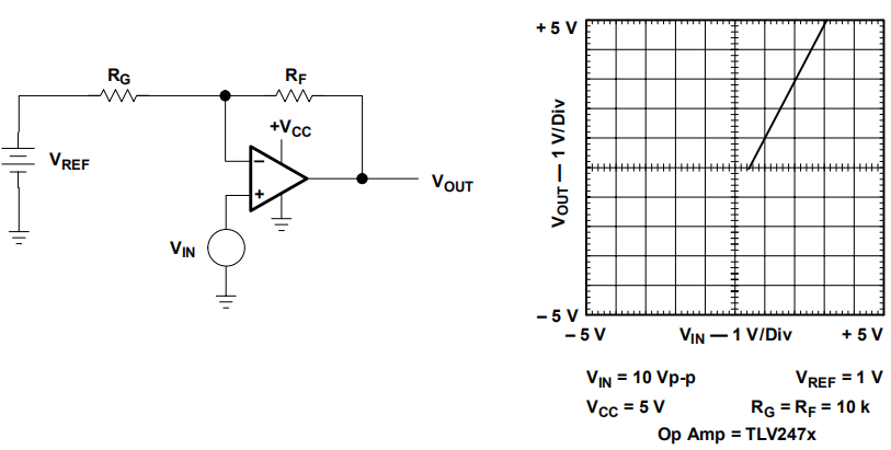
Figure A–9. Noninverting Op Amp with Inverting Positive Reference
6. Noninverting Op Amp with Noninverting Negative Reference
The transfer equation takes the form of Y = mX – b and is given in Equation A–6.

The transfer function slope is positive, and the dc intercept is negative. The reference is terminated in R1 and R2. R1 and R2 can be selected independent of RF and RG to obtain the desired slope and dc intercept. The price for the extra degree of freedom is two resistors.

Figure A–10. Noninverting Op Amp with Noninverting Negative Reference
7. Noninverting Op Amp with Inverting Negative Reference
The transfer equation takes the form of Y = mX + b and is given in Equation A–7.

The transfer function slope is positive, and the dc intercept is positive. This is the minimum component count configuration for this transfer function. The reference termination resistor is connected to a virtual ground, so RG is the load across VREF. RF and RG are contained in both halves of the equation. Thus it is hard to obtain the desired slope and dc intercept without modifying VREF or placing an attenuator in series with VIN.

Figure A–11. Noninverting Op Amp with Inverting Positive Reference
8. Noninverting Op Amp with Noninverting Positive Reference
The transfer equation takes the form of Y = mX + b and is given in Equation A–8.

The transfer function slope is positive, and the dc intercept is positive. The reference is terminated in R1 and R2. R1 and R2 can be selected independent of RF and RG to obtain the desired slope and dc intercept. The price for the extra degree of freedom is two resistors.

Figure A–12. Noninverting Op Amp with Noninverting Positive Reference
9. Differential Amplifier
When RF is set equal to R2 and RG is set equal to R1, Equation A–9 reduces to Equation A–10.

These resistors must be matched very closely to obtain good differential performance. The mismatch error in these resistors reduces the common-mode performance, and the mismatch shows up in the output as an amplified common-mode voltage. Consider Equation A–10. Note that only the difference signal is amplified, thus this configuration is called a differential amplifier. The differential amplifier is a popular circuit in precision applications where it is used to amplify sensor outputs while rejecting common mode noise.
The inverting input impedance is RG because of the virtual ground at the inverting op amp input. The noninverting input impedance is RF + RG because the noninverting op amp input impedance approaches infinity. The two input impedances are different, and this leads to two problems with this circuit.
First, mismatched input impedances preclude any attempts to cancel input bias currents through resistor matching. Often R2 is set equal to RF || RG so that the bias currents develop equal common-mode voltages which the op amp rejects. This is not possible when R2 = RF and R1 = RG unless the source impedances are matched. Second, high output impedance sensors are often used, and when high output sensors work into mismatched input impedances, errors occur.

Figure A–13. Differential Amplifier
10. Differential Amplifier With Bias Correction
When RF is set equal to R2 and RG is set equal to R1, Equation A–11 reduces to Equation A–12.

When an offset voltage must be eliminated from or added to the input signal, this differential amplifier circuit is employed. The reference voltage can be positive or negative depending upon the polarity offset required, but care must be taken to protect the op amp inputs and not exceed the output range.

Figure A–14. Differential Amplifier with Bias Correction
11. High Input Impedance Differential Amplifier
When RF is set equal to R1 and RG is set equal to R2, Equation A–13 reduces to Equation A–14.

Each input signal is connected to an op amp noninverting input that is very high impedance. The input impedance of the circuit is very high, and it is matched, so this circuit is often used to interface to high-impedance sensors. Each op amp has a signal propagation time, and VIN1 experiences two propagation delays versus VIN2’s one propagation delay.
At high frequencies, the propagation delay becomes a significant portion of the signal period, and this configuration is not usable at that frequency.
RF and R2, and RG and R1 should be matched to achieve good common-mode rejection capability. Bias current cancellation resistors equal to RF || RG should be connected in series with the input sources for precision applications.

Figure A–15. High Input Impedance Differential Amplifier
12. High Common-Mode Range Differential Amplifier
When all resistors are equal, Equation A–15 reduces to Equation A–16.

R1 and RG2 are equal-value resistors terminated into a virtual ground, hence, the input sources are equally terminated. This configuration has high common-mode capability because R1 and RG2 limit the current that can flow into or out of the op amp. Thus, the input voltage can rise to any value that does not exceed the op amp’s drive capability. The voltage references, VREF1 and VREF2, are added for bias purposes. Without bias, the output voltage of the op amps would saturate at ground, and the bias voltages keep the output voltage of the op amp positive.

Figure A–16. High Common-Mode Range Differential Amplifier
13. High-Precision Differential Amplifier
When R7 = R6, R5 = R2, R1 = R4, and VREF1=VREF2, Equation A–17 reduces to Equation A–18.

In this circuit configuration, both sources work into the input impedance of a noninverting op amp. This impedance is very high, and if the op amps are identical, both impedances are very nearly equal. The propagation delay is still equal to two op amp propagation delays, but the propagation delay is very nearly equal, so any distortion resulting from unequal propagation delays is minimized.
The equal resistors should be matched with more precision than is expected from the circuit. Resistor matching eliminates distortion due to unequal gains, and it reduces the common-mode voltage feed through. Resistors equal to (R1 || R3)/2 may be placed in series with the sources to reduce errors resulting from bias currents. This differential amplifier has the unique feature that the gain can be changed with only one resistor, and if the gain setting resistor is R3, no resistor matching is required to change gain.
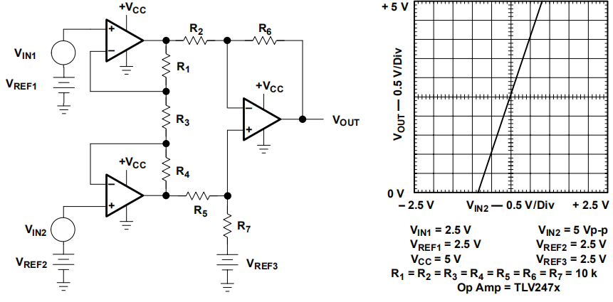
Figure A–17. High-Precision Differential Amplifier
14. Simplified High-Precision Differential Amplifier
When RF is set equal to R2, RG is set equal to R1, and VREF1 = VREF2, Equation A–19 reduces to Equation A–20.

Both input sources are loaded equally with very high impedances in the simplified high precision differential amplifier. This configuration eliminates three resistors, two of which are matched, but it sacrifices flexibility in gain setting capability because the gain must be set with a matched pair of resistors.

Figure A–18. Simplified High-Precision Differential Amplifier
15. Variable Gain Differential Amplifier
When R1 is set equal to R3 and R2 is set equal to R4, Equation A–21 reduces to Equation A–22.

When a function is enclosed in a feedback loop, the function acts inverted on the closed loop transfer function. Thus, the gain stage RF/RG ends up being an attenuator. The circuit shown in Figure A–19 can be used with any of the differential amplifiers to change gain without affecting matched resistors. R1, R3 and R2, R4 must be matched to reduce the common-mode voltage.

Figure A–19. Variable Gain Differential Amplifier
16. T Network in the Feedback Loop
Sometimes it is desirable to have a low-resistance path to ground in the feedback loop. Standard inverting op amps cannot do this when the driving circuit sets the input resistor value and the gain specification sets the feedback resistor value. Inserting a T network in the feedback loop yields a degree of freedom that enables both specifications to be met with a low dc resistance path to ground in the feedback loop.


Figure A–20. T Network in the Feedback Loop
17. Buffer
The buffer input signal polarity must be unipolar because the output voltage swing is unipolar. When this limitation precludes the buffer, a differential amplifier with the negative input correctly biased is used, or a reference voltage is added to the buffer to offset the output voltage. RF must be included when the op amp inputs are not rated for the full supply voltage. In that case, RF limits the current into the op amp inputs, thus preventing latch up. Most new op amp inputs can withstand the full supply voltage, so they often leave RF out as cost savings. The main attraction of the buffer is that it has very high input impedance and very low output impedance. The impedance transformation capability is why buffers are often added to the input of other circuits.

Figure A–21. Buffer
18. Inverting AC Amplifier
VCC and resistors R set a dc level of VCC/2 at the inverting input. RG is connected to ground through a capacitor, thus the circuit functions as a buffer for dc. This causes the dc output voltage to be VCC/2, so the quiescent output voltage is the middle of the supply voltage, and it is ready to swing to either rail as the input signal commands.
The ac gain is given in Equation A–25. RG and C form a coupling network for the ac signal. Good coupling networks should be constant low impedance at the signal frequencies, so Equation A–26 should be satisfied to get good low-frequency performance. The lowest frequency component of the input signal, fMIN, is determined by completing a Fourier series on the input signal. Then, setting fMIN = 100f in Equation A–26 ensures that the 3-dB breakpoint introduced by RG and C is two decades lower than fMAX.


Figure A–22. Inverting AC Amplifier
19. Noninverting AC Amplifier
VCC and the resistors (R) set a dc level of VCC/2 at the inverting input. RG is connected to ground through a capacitor, thus the circuit functions as a buffer for dc. This causes the dc output voltage to be VCC/2, so the quiescent output voltage is the middle of the supply voltage, and it is ready to swing to either rail as the input signal commands.
The ac gain is given in Equation A–27. RG and C create a coupling network for the ac signal. Good coupling networks should be a constant low impedance at the signal frequencies, so Equation A–28 should be satisfied to get good low frequency performance. The lowest frequency component of the input signal, fMIN, is determined by completing a Fourier series on the input signal. Then, setting fMIN = 100f in Equation A–28 ensures that the 3-dB breakpoint introduced by RG and C is two decades lower than fMAX. The breakpoint for RG and C1 is set in a similar manner.

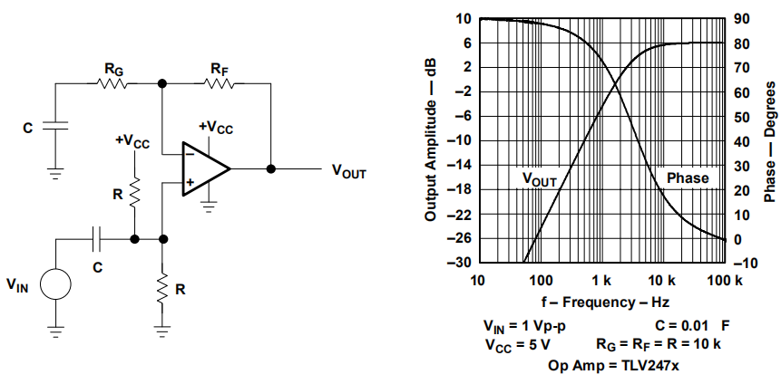
Figure A–23. Noninverting AC Amplifier
Computing Circuits
Four versions of the inverting op amp and four versions of the noninverting op amp were given in the previous section. During the concept stage of the design, one of these eight op amp circuits is selected. Specifications for the input and output voltage are the selection criteria that determines which circuit configuration is used.
There are four versions of most of the circuits given in this and following sections, but just the simplest version of any circuit is included in this appendix because of space limitations. Each circuit configuration can be modified as required to fit specific applications.
Look back to the first section to determine what bias is required to fit the application, and adapt that bias to the new circuit.
1. Inverting Summer
The three input voltages are inverted and added as Equation A–29 shows. RB should be made equal in value to the parallel combination of RF, RG1, RG2, and RG3 to convert the input bias current to a common-mode voltage so the op amp can reject it. VREF sets the output voltage somewhere between the supply limits, and this allows negative addition (subtraction) to take place.


Figure A–24. Inverting Summer
2. Noninverting Summer
This circuit adds the input voltages and multiplies them by the stage gain. RG1, RG2, and RG3 in parallel should be equal to RF in parallel with RG to cancel the input bias current using the common-mode input voltage rejection technique. VREF is added to the circuit to enable the addition of negative values.


Figure A–25. Noninverting Summer
3. Noninverting Summer with Buffers
VREF1 and VREF2 are added to enable the buffers to handle positive input voltages. Their output contribution to the last stage is cancelled out by VREF3. This configuration uses fewer resistors at the expense of two op amps. RG1, RG2, and RF in parallel should be made equal to RB to cancel the input bias current.


Figure A–26. Noninverting Summer with Buffers
4. Inverting Integrator
The Laplace operator, s= jω, is used in Equation A–32, and the mathematical operation 1/s constitutes an integration. Differentiation circuits are shown later, and the mathematical operation, s, constitutes a differentiation. The integration time constant is RC, thus the magnitude crosses 0 dB on a log plot when RC = 1. Also the phase is –45° when RC = 1.

This integrator is not very practical because there is no method of discharging the capacitor; hence, any leakage current will eventually charge the capacitor until the circuit becomes saturated. The positive input of the integrator is biased at VCC / 2 to center the output voltage at VCC / 2; thus allowing for positive and negative voltage swings. The bias resistors are selected as 2R so that the parallel combination equals R. This offsets the input current drawn through R.

Figure A–27. Inverting Integrator
5. Inverting Integrator with Input Current Compensation
Functionally, this circuit is the same as that shown in Figure A–27, but a current compensation network has been added to offset the input current. VCC, R1, and R2 bias the positive input at VCC / 2 to center the output voltage at VCC / 2; thus allowing for positive and negative voltage swings.
R1 and R2 are selected as relatively small values because the current flowing through RA also flows through the parallel combination of R1 and R2. RA forward biases the diode with a constant current, thus the diode acts like a small voltage regulator. The diode voltage drop is temperature sensitive, and this factor works in our favor because the input transistors are temperature sensitive. The two temperature sensitivities cancel out if the diode current is selected correctly. RB is a large-value resistor that acts like a current source, so it is selected such that it supplies the input bias current. Selecting RB correctly ensures that no input current flows through the integration resistor, R.
This integrator is not very practical because there is no method of discharging the capacitor. Hence, any input current will eventually charge the capacitor until the circuit becomes saturated. The bias circuit drastically reduces the input current flowing through R, thus it extends the integration time. A reset circuit is needed to make the integrator more practical.
This bias compensation scheme is set up for an op amp that has NPN input transistors. The diode must be reversed and connected to ground for op amps with PNP input circuits.

Figure A–28. Inverting Integrator with Input Current Compensation
6. Inverting Integrator with Drift Compensation
Functionally, this circuit is the same as that shown in Figure A–27, but it uses an RC circuit in the positive lead to obtain drift compensation. The voltage divider is made from a series string of resistors (RA), and VCC biases the input in the center of the power supply. Positive input current flows through R and C in parallel, so the positive input current drops the same voltage across the parallel RC combination as the negative input current drops across its series RC combination. The common-mode rejection capability of the op amp rejects the voltages caused by the input currents. Much longer integration times can be achieved with this circuit, but when the input signal does not center around VCC/2, the compensation is poor.


Figure A–29. Inverting Integrator with Drift Compensation
7. Inverting Integrator with Mechanical Reset
Functionally, this circuit is the same as that shown in Figure A–27, but a method has been provided to discharge (reset) the capacitor. S1 is a mechanical switch or relay and when the contacts close, they short the integrating capacitor forcing it to discharge. Some capacitors are sensitive to fast discharge cycles, so RS is put in the discharge path to limit the initial discharge current. When RS is absent from the circuit, the impulse of current that occurs at the first instant of discharge causes considerable noise, so the selection of RS is also based on noise considerations. For all practical purposes, the time constant formed by RS and C determines the discharge rate.
One advantage of mechanical discharge methods is that they are isolated from the remainder of the circuit. Their size, weight, time delay, and uncertain actuating time offset this advantage. When the disadvantages of mechanical reset outweigh the advantages, circuit designers go to electronic reset circuits.


Figure A–30. Inverting Integrator with Mechanical Reset
8. Inverting Integrator with Electronic Reset
Functionally, this circuit is the same as that shown in Figure A–27, but an electronic method has been provided to discharge (reset) the capacitor. Q1 is controlled by a gate drive signal that changes its state from on to off. When Q1 is on, the gate-source resistance is low, less than 100 Ω. Αnd when Q1 is off, the gate-source resistance is high — about several hundred MΩ.
The source of the FET is at the inverting lead that is at ground, so the Q1 gate-source bias is not affected by the input signal. Sometimes, the output signal can get large enough to cause leakage currents in Q1, so the designer must take care to bias Q1 correctly. Consult a transistor book for more detailed information on transistor reset circuits. A major problem with electronic reset is the charge injected through the transistor’s stray capacitance.
This charge can be large enough to cause integration errors.


Figure A–31. Inverting Integrator with Electronic Reset
9. Inverting Integrator with Resistive Reset
This circuit differs from that shown in Figure A–27 because it yields a breakpoint rather than a pure integration. On a log plot, the integrator slope is –6 dB per octave at the 0 frequency intercept, and the 0 dB intercept occurs when f = 1/2πRC. A breakpoint plots flat on a log plot until the breakpoint where it breaks down at –6 dB per octave. It is –3 dB when f = 1/2πRC.
RF is in parallel with the integrating capacitor, C, so it is continually discharging C. The low frequency attenuation that is the best attribute of the pure integrator is sacrificed for the reset circuit complexity.


Figure A–32. Inverting Integrator with Resistive Reset
10. Noninverting Integrator with Inverting Buffer
This circuit is an inverting integrator preceded by an inverting buffer. Eliminating the signal inversion costs an op amp and four resistors, but this is the easiest way to get true noninverting integrator performance.


Figure A–33. Noninverting Integrator with Inverting Buffer
11. Noninverting Integrator Approximation
This circuit has fewer parts than the Noninverting Integrator With Inverting Buffer (Figure A–33), but it is not a true integrator because there is a zero in the transfer equation. The log plot starts rolling off at a –6 dB per octave rate at low frequencies, but when f = 1/2πRC, the zero cuts in. The zero causes the log plot to flatten out because the slope decreases to 0 db per decade.
This circuit functions as an integrator at very low frequencies, but at frequencies higher than f = 1/2πRC, it functions as a buffer.


Figure A–34. Noninverting Integrator Approximation
12. Inverting Differentiator
The log plot of the differentiator is a positive slope of 6-dB per octave passing through 0 dB at f = 1/2πRC. At extremely high frequencies, the capacitive reactance goes to very low values, thus the circuit gain approaches the op amp open-loop gain. This performance emphasizes any system noise or noise generated by the op amp. The poor noise performance of this circuit limits its application to a very few specialized situations.
This configuration has a pole in the feedback loop. If the op amp has more than one pole, and most op amps have several poles, this configuration can become oscillatory. The VCC and RA circuit bias the output in the center of the power supplies. RA/2 should be selected equal to RG||RF so that input currents are canceled out.

Figure A–35. Inverting Differentiator
13. Inverting Differentiator with Noise Filter
This circuit has a pure differentiator that rises at a 6-dB per octave slope from zero frequency. At f = 1/2πRFCF, the pole kicks in and the slope is reduced to zero. The pole has two effects. First, it stabilizes the circuit by canceling zero’s phase shift. Second, it limits the circuit gain to 1 at high frequencies, so it acts like a noise filter. R/2 should equal RF for good input current cancellation, and VCC coupled with R centers the output voltage.


Figure A–36. Inverting Differentiator with Noise Filter
Oscillators
Some general op amp sinewave oscillator circuits that fall under three main categories: Wien bridge, phase shift, and quadrature. A brief description and of each type is provided, along with one or two variations. Op amp sinewave oscillators are used to create references in applications such as audio and function/waveform generators.
1. Basic Wien Bridge Oscillator
When ω = 2πf = 1/RC, the feedback is in phase (this is positive feedback), and the gain is 1/3, so oscillation requires an amplifier with a gain of 3. When RF = 2RG the amplifier gain is 3 and oscillation occurs at f = 1/2πRC. Normally, the gain is larger than 3 to ensure oscillation under worst case conditions.
VREF sets the output dc voltage in the center of the span. The output sine wave is highly distorted because limiting by saturation and cutoff is controlling the output voltage excursion. The distortion decreases when the gain is decreased, but the circuit may not oscillate under worst-case low gain conditions.


Figure A–37. Basic Wien Bridge Oscillator
2. Wien Bridge Oscillator with Nonlinear Feedback
When the circuit gain is 3, RL = RF/2.
Substituting a lamp (RL) for the gain setting resistor reduces distortion because the non– linear lamp resistance adjusts the gain to keep the output voltage smaller than the power supply voltage. The output voltage never approaches the power supply rail, so distortion doesn’t occur. RF and RL determine the lamp current (see Equations A–43 and A–44).

The lamp is selected by examining lamp resistance curves until a lamp with a resistance approximately equal to RF/2 at IOUT(RMS) is found. The output voltage swing should be less than 75% of the maximum guaranteed voltage swing, and 3 RL must be greater than the load resistance specified for the voltage swing specification. VREF should be VCC/5.

Figure A–38. Wien Bridge Oscillator with Nonlinear Feedback
3. Wien Bridge Oscillator with AGC
The op amp is configured as an ac amplifier to ease biasing problems. The gain equation for the op amp is given below. RG1 or RG2, but not both resistors, is required depending on the selection of the Q1.
The diode, D1, half-wave rectifies the output voltage and applies it to the voltage divider formed by R1 and R2. The voltage divider biases Q1 in its linear region, and they eventually set the output voltage. C1 filters the rectified sine wave with a long time constant so that the output voltage stays constant. C2 must be selected large enough to act as a short at the oscillation frequency.
As the output voltage increases, the negative voltage across the gate of Q1 increases. The increased negative gate voltage causes Q1 to increase its drain-to-source resistance. This results in increased op amp gain and an output voltage decrease. When the voltage divider and FET are selected properly, the output voltage swing is less than the guaranteed maximum swing, so distortion doesn’t occur.


Figure A–39. Wien Bridge Oscillator with AGC
4. Quadrature Oscillator
Quadrature oscillators produce sine waves 90° out of phase, so they output sine/cosine, or quadrature waves.
When R1C1 = R2C2 = R3C3, the circuit oscillates at ω = 2πf = 1/RC. Both op amps act as integrators causing two poles at 1/RC, thus the circuit oscillates when the loop gain crosses the 0-dB axis. The integrators ensure that gain is always sufficient for oscillation. There is a slight bit of distortion at the sine output, and it is very hard to eliminate this distortion.

Figure A–40. Quadrature Oscillator
5. Classical Phase Shift Oscillator
Theoretically, the three RC sections do not load each other, thus the loop gain has three identical poles multiplied by the op amp gain. The loop phase shift is –180° when the phase shift of each section is –60°, and this occurs when ω = 2πf = 1.732/RC because the tangent of 60° = 1.73. The magnitude of β at this
point is (1/2)3, so the gain, A = RF/RG, must be greater or equal to 8 for the system gain to be equal to 1.
The assumption that the RC sections do not load each other is not entirely valid, thus the circuit does not oscillate at the specified frequency, and the gain required for oscillation is more than 8. This circuit configuration was very popular when an active component was large and expensive, but now that op amps are inexpensive, small, and come quad packages, the classical phase shift oscillator is losing popularity.
The classical phase shift oscillator has an undistorted sine wave available at the output of the third RC section. This is not a low-impedance output, and the signal amplitude is smallest here, but these sacrifices have to be made to get away from distortion. An undistorted output can be obtained from the op amp if an AGC circuit similar to the one shown in Figure A–39 is employed. The reference voltage is set according to the equation VREF = VCC/ 2(1+RF/RG) to center the output voltage at VCC/2.


Figure A–41. Classical Phase Shift Oscillator
6. Buffered Phase Shift Oscillator
A noninverting op amp buffers each RC section in this oscillator. Equation A–46, repeated below, truly represents the transfer function of this circuit if RG >> R.

The loop phase shift is –180° when the phase shift of each section is –60°, and this occurs when ω = 2πf = 1.732/RC because the tangent 60° = 1.73. The magnitude of β at this point is (1/2)3, so the gain, A = RF/RG, must be greater or equal to 8 for the system gain to be equal to one.
The buffered phase shift oscillator has an undistorted sine wave available at the output of the third RC section. This is not a low-impedance output, and the signal amplitude is smallest here, but these sacrifices have to be made to get away from distortion. An undistorted output can be obtained from the op amp if an AGC circuit similar to the one shown in Figure A–39 is employed.
There are three op amps, so the gain can be distributed among the op amps at the expense of a few resistors, and the distortion is reduced. Another method of reducing distortion is to limit the output voltage swing softly with external components. The limiting technique does not yield as good results as the AGC technique does, but it is less expensive.
The reference voltage is set according to the equation VREF = VCC/ 2(1+RF/RG) to center the output voltage at VCC/2.

Figure A–42. Buffered Phase Shift Oscillator
7. Bubba Oscillator
The Bubba oscillator is another phase shift oscillator, but it takes advantage of the quad op amp package to yield some unique advantages. Each RC section is buffered by an op amp to prevent loading. When RG >> R there is no loading in the circuit, and the circuit yields theoretical performance.
Four RC sections require –45° phase shift per section to accumulate –180° phase shift. Each RC section contributes –45° phase shift when ω = 1/RC. The gain required for oscillation is G ≥ (1/0.707)4 = 4. Taking outputs from alternate sections yields low-impedance quadrature outputs. When an output is taken from each op amp, the circuit delivers four 45° phase-shifted sine waves.
The gain, A, must equal 4 for oscillation to occur. Very low distortion sine waves can be obtained from the junction of R and RG. When low-distortion sine waves are required at all outputs, the gain should be distributed among the op amps. Gain distribution requires biasing of the other op amps, but it has no effect on the oscillator frequency. This oscillator has the best dφ/df of the phase shift oscillators, so it has minimum frequency drift. The reference voltage is set according to the equation VREF = VCC/ 2(1+RF/RG) to center the output voltage at VCC/2.


Figure A–43. Bubba Oscillator
8. Triangle Oscillator
The triangle oscillator produces triangle waves and square waves. The op amp functions as an integrator. When the output voltage of the comparator is low, the output of the op amp charges C until the output voltage exceeds the hysteresis voltage set by R1 and RF and the reference voltage (VCC/2). At this point, the comparator output switches to a high state and the op amp integrates the voltage in a negative direction. The triangle wave (op amp output voltage swing) is given in Equation A–49. The frequency of oscillation is given in Equation A–50.

The op amp reference voltage can be adjusted to equalize the triangle rise and fall times.

Figure A–44. Triangle Oscillator
No comments:
Post a Comment