Introduction to Designing Low-Voltage Op Amp Circuits
In one respect, voltage is like water: you don’t appreciate its value until your supply runs low. Low-voltage systems, defined here as a single power supply less than 5 V, teach us to appreciate voltage. We aren’t the first electronic types to learn how valuable voltage is; about 15 years ago the audio console design engineers appreciated the relationship between voltage and dynamic range. They needed more dynamic range to satisfy their customers; thus, they ran op amps at the full rated voltage, not the recommended operating voltage, so they could squeeze a few more dB of dynamic range from the op amp.
These engineers were willing to take a considerable risk running op amps at the full rated voltage; but their customers demanded more dynamic range. The moral of this story is that dynamic range is an important parameter, and supply voltage is tied directly to dynamic range. Knowing how to obtain and use the maximum dynamic range and input/output voltage range is critical to achieving success in low voltage design. We will investigate these subjects in detail later, but for now it is useful to review the history of op amps. Knowing how op amps evolved into the today’s marvels is interesting, and it gives designers an insight into system problems that they encounter as they design in the low voltage world.
When power supplies were ±15 V, the output voltage swing of an op amp didn’t seem important. When the power supply was 30 V the typical circuit designer could afford to sacrifice 3 V from each end of the output voltage swing (this was because of transistor saturation or cutoff). The transistors in the op amp need enough voltage across them to operate correctly, so why worry about 6 V out of 30 V. Also, the input transistors required base bias, so an op amp with 30-V supplies often offered a common-mode input voltage range of 24 V or less. These numbers come from the µA741 data sheet; the µA741 (about 1969) is the first internally compensated op amp to achieve wide popularity.
A later generation op amp, the LM324, had better dynamic range characteristics than the µA741. The LM324’s output voltage swing is 26 V when operated from a 30-V power supply, and the common-mode input voltage range is 28.5 V. The LM324 was big news because it was specified to operate with a 5-V power supply. The LM324’s output voltage swing at VCC = 5 V is 3.48 V, and this presented problems for the early low voltage circuit designers because the output voltage swing was smaller than most analog-to-digital converter (ADC) input voltage ranges. You must fill the ADC input voltage range to obtain its full dynamic range. The LM324 had an input voltage common-mode range of (VCC–1.5 V) to 0 V; at least this op amp could work with transducers connected to the lower power supply rail if the transducer did not have an ac output voltage swing.
The next incremental improvement in op amps was the LM10 because it operated on 1.1-V power supplies. It was introduced almost as an afterthought because there was no pressing demand for it. Its brilliant designer, Robert J. Widlar, wrote “IC op amps have reached a certain maturity in that there no longer seems to be a pressing demand for better performance.” There were no pressing demands for a low voltage op amp in 1978 because portable (portable means battery applications that are almost always single supply) did not become popular until the late 1980s or early 1990s.
Cell phones, calculators, and portable instruments — not new battery technology — opened the market for low-voltage op amps, and when the portable concept caught on, the demand for low-voltage op amps increased. The increasing demand did not breed new companies committed to low-voltage IC design; rather, the established IC manufacturers threw a few low voltage op amps into their portfolio. These op amps, like the LM324, could operate on a low voltage, but they were severely lacking in input common-mode voltage range and output voltage swing. Circuit designers had to be satisfied with this generation of op amps until something better came along. Well, something better is here now!
The next generation of low-voltage op amps has much better specifications. The TLV278X operates off a power supply ranging from 1.8 V to 3.6 V, and it has an output voltage swing of 1.63 V (when the power supply is 1.8 V) coupled with an input common mode voltage range of –0.2 V to 2 V. The TLV240X operates off a power supply ranging from 2.5 V to 16 V, and it has an output voltage swing of 2.53 V when the power supply voltage is 2.7 V. Also, when it is operated off a 2.7-V power supply, it has an input common mode voltage range of –0.1 V to 7.7 V. These new op amps are far superior to their predecessors when evaluated on the their merits, which are extended output voltage swing and input common voltage range.
The latest op amps make it possible to design more accurate and cost effective electronic equipment, but there is one problem that they don’t solve. Low-voltage applications are defined here as single-supply applications, and in single-supply design, the op amp input voltage and output voltage is referenced to the midpoint of the power supply (VCC/2). Unfortunately, most transducers are not connected to the midpoint of the power supply because, in the majority of cases, this requires a third wire beyond VCC and ground. It doesn’t help to create VCC/2 at the transducer location (to save a wire) because it is not identical to the midpoint of the power supply (unresolved errors enter because of the reference voltage difference). When the transducer in a single supply design is referenced to any voltage other than the midpoint of the power supply, the reference voltage is amplified with the transducer voltage.
The trick to designing single supply op amp circuits is using external biasing to strip off or null out the reference voltage. Designing op amp circuits with biasing normally involves an iterative cut and try approach where the designer assumes a circuit configuration, solves equations, changes the configuration, and repeats the process until a solution is found. A technique that solves the problem the first time is presented later.
Dynamic Range
It is extremely hard to define dynamic range (DR) for an op amp, so lets start with a digital to-analog converter (DAC) where DR is defined as the ratio of the maximum output voltage to the smallest output voltage the DAC can produce (least significant bit or LSB). Dynamic range is usually expressed in dB using the formula given in Equation 18–1.
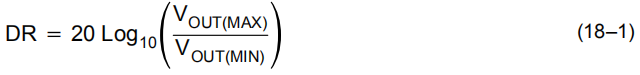
The same definition of DR can be used for an op amp, and the maximum output voltage swing equals VOUTMAX. This output voltage swing is defined as the maximum output voltage the op amp can achieve (VOH) minus the minimum output voltage the op amp can achieve (VOL). VOH and VOL are easily obtainable from an op amp IC data sheet. Normally, VOH and VOL are guaranteed minimum and maximum parameters respectively. This yields Equation 18–2.
Equation 18–2 can be used to illustrate the role that power supply voltage plays in limiting the DR. VOH(MIN) is the most positive power supply voltage minus the voltage drop across the upper output transistor, thus VOH(MIN) is directly proportional to the most positive power supply voltage. For any op amp, the output voltage swing is directly proportional to the power supply voltage, thus, in the same op amp, the DR is directly proportional to the power supply voltage.
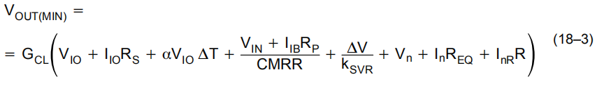
At first thought, one might think that the smallest output voltage that an op amp can have is zero, and the natural conclusion based on this assumption is that the DR is equal to infinity. This is never the case because op amp and external circuit imperfections ensure that the smallest op amp output voltage is greater than zero. It turns out that VOUT(MIN) is actually determined by a series of error terms. These error terms are the op amp’s internal noise (Vn and In), external resistor noise (VnR), power supply rejection ratio (kSVR), voltage offset (VIO), current offset (IIO), common-mode rejection ratio (CMRR), and closed loop gain (G). Each of these error terms is referred to the input of the op amp, so they must be multiplied by the closed loop gain to be referred to the output (see Figure 18–1).

Figure 18–1. Op Amp Error Sources
The error sources are taken into account in Equation 18–3, and this equation refers them to the op amp output by multiplying them by the op amp’s closed loop gain.
The maximum DR that can be achieved by an op amp is given in Equation 18–4.

The DR is reduced by the sum of the error terms, so it is proper to conclude that the maximum power supply voltage and the op amp choice (this defines the error magnitude) both establish the DR of an op amp. The first two terms in Equation 18–3 are dc error terms, thus, they can be adjusted to zero by one of several methods not mentioned here. The input offset current and input bias current error terms were big factors with older generation ICs, but today’s technology render them much less significant (see Table 18–1).
Table 18–1. Comparison of Op Amp Error Terms
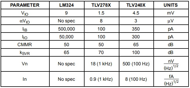
The data in Table 18–1 indicates that older low voltage op amps are not capable of yielding the DR that that later technology op amps are.
Signal-to-Noise Ratio
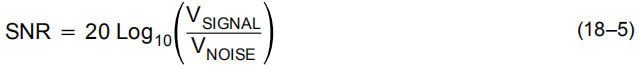
Noise sets a limit on the information and signals that can be handled by a system. The ability of an amplifier, receiver, or other device to discern a signal is degraded by noise. Noise mixed with the incoming signal, noise generated by the op amp, resistor noise, and power supply noise ultimately determine the size of the signal that can be recovered and measured.
Noise fluctuates randomly over a period of time, so instantaneous signal or noise levels don’t describe the situation adequately. Averages over a long period of time (root mean squared or RMS) are used to describe both the signal and the noise. Signal-to-noise ratio (SNR) was initially established as a measure of the quality of the signal that exists in the presence of noise. This SNR was a power ratio, and it was established at the output of a circuit. The SNR that we are interested in is a voltage ratio because the impedance is constant, and it is established at the input to the op amp. This means that all noise voltages, including resistor noise voltage, must be calculated in RMS volts at the op amp input. The SNR is given in Equation 18–5.
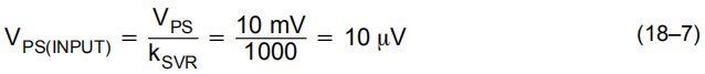
The signal is established by a transducer; a device that senses a change in a variable and converts that change into a voltage change. Transducers also convert some of their physical surroundings into a noise voltage that is combined with the signal. Noise from the physical surroundings of the transducer, unless its nature is well known, is almost impossible to separate from the transducer signal. When transducers are connected to the electronics, cabling picks up noise, and some transducers like thermocouples can pick up noise from the connecting junctions. Thus, the signal is never clean as it enters the electronics. The noise generated by the op amp was defined in the previous section as Vn, InREQ, InRR, and ∆V/kSVR, and this noise is added to the signal. The transducer often has a very small output voltage swing, so when the transducer output voltage swing is converted to least significant bits (LSB) the noise voltage should be very small compared to an LSB. Consider a temperature transducer that has a 10-mV
swing over its range. When the transducer output voltage swing is considered to be the full-scale voltage (FSV) of an ADC, the LSB is very small as is shown in Equation 18–6 for a 12-bit (N) ADC.

The op amp for this application must be a very low noise op amp because an op amp with a 20-nV/(Hz)1/2 equivalent input noise voltage and a bandwidth of 4 MHz contributes 40 µV of noise. This high noise contribution is why extensive filtering and “optimally” low bandwidth is found desirable in the input stages of some electronic systems. If there is power supply noise, some of that noise passes through the op amp to its input. The power supply noise is divided by the power supply rejection ratio, but there is always a residual noise component of the power supply on the op amp input as shown in Equation 18–7 where kSVR is 60 dB.
Input Common-Mode Range
Years ago the op amp’s input common-mode voltage range (VICR) did not include the power supply rails. The best VICR that was available was (VCC +|VEE|–6 V), and when the input voltage approached VICR, distortion occurred. If the input voltage exceeded the power supply rails, the output stage might invert phase (it sometimes latched in the inverted position causing control problems) or the IC might self destruct. The vast majority of transducers were connected to ground (0 V) because it was easy to make a ground connection and because a split supply op amp has inputs referenced to ground. In a split supply application with the transducer connected to ground, latch-up or self destruction is unlikely.
In special cases, transducers are connected to a power supply rail (usually VCC when power supply current sensing) or some other voltage, and in this special case, additional bias circuitry was added to split power supply designs to keep the input voltage swing within VICR. Bias circuitry in conjunction with external components removed the effects of the power supply rail connection.
Many low voltage op amp input signals come from transducers connected to a power supply rail like the circuit shown in Figure 18–2.
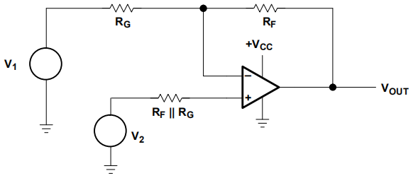
Figure 18–2. Noninverting Op Amp
When V1 = 0 and V2 is the transducer input, the op amp must be capable of handling input voltages that go to 0 V. Furthermore, the transducer voltage may be ac, so it swings above and below ground, thus the transducer voltage drops below the low power supply rail. This situation requires that the op amp’s VICR exceed the power supply voltage. Rail-to-rail input (RRI) voltage capability is a necessary requirement for a low-voltage op amp that handles transducers connected to a power supply rail.
When the input voltage is connected to ground and the input voltage swing is very small, a standard op amp like the LM324 suffices. Referring to Figure 18–3 it can be seen that the PNP input transistors are biased by the emitter current source. If the positive input is connected to ground bias current still flows and the transistor stays active. If the input transistors are selected very carefully for operation with low collector-base junction reverse bias, the input voltage can go slightly below ground (–200 mV for the TLV278X) and the op amp will still operate correctly. The circuit operation is one sided though because when the input voltage approaches the positive supply rail, the emitter current source and input transistors turn off. This type of circuit does not offer rail-to-rail operation, but it does offer from rail to (VCC –1.5V) operation.
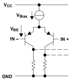
Figure 18–3. Input Circuit of a NonRRI Op Amp
An op amp with a NPN input stage works in a similar way around the positive supply rail. It can sense voltages close to VCC and maybe slightly above VCC, but it won’t work when it is within 1.5 V of ground. The solution for this problem is to include parallel input circuits as shown in Figure 18–4.
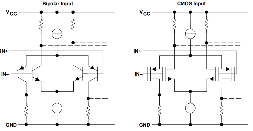
Figure 18–4. Input Circuit of an RRI Op Amp
The RRI op amps have parallel input stages. There are both PNP and NPN differential amplifiers used in the input stages of the RRI op amp, thus the RRI op amp can operate above and below the power supply voltage. As Figure 18–4 shows, the parallel input stages can be made in bipolar or MOS technology.
The input stages operate in three different ranges. When the input voltage ranges from about –0.2 V to 1 V, the PNP differential amplifier is active and the NPN differential amplifier is cutoff. When the input voltage ranges from about 1 V to (VCC –1 V), both the NPN and PNP differential amplifiers are active. When the input voltage ranges from about (VCC –1 V) to (VCC + 0.2 V), the NPN differential amplifier is active and the PNP differential amplifier is cut off. Inclusion of complementary differential input amplifiers achieves VICR exceeding the power supply limits, but there is a penalty to pay in input bias current, input offset voltage, and distortion. Figures 18–5 and 18–6 show the input bias current and input offset voltage as a function of the input common-mode voltage.
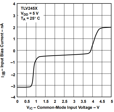
Figure 18–5. Input Bias Current Changes with Input Common-Mode Voltage

Figure 18–6. Input Offset Voltage Changes with Input Common-Mode Voltage
When both transistors are conducting current the input bias currents have a tendency to cancel, so in the range of ±1 V, the bias current is extremely low even when bipolar transistors are used to make the op amp. Above this range, the PNP differential amplifier cuts off so the full bias current requirement of the NPN transistor becomes apparent. The same action happens below this range when the NPN differential amplifier cuts off. Notice that the PNP bias current is significantly larger than the NPN bias current; this is expected because NPN transistors have better gain characteristics than PNP transistors. The base emitter voltage of the NPN and PNP transistors is well matched because the magnitude of the input offset voltage at the extremes is almost equal. The bias current and offset voltage variation with input signal amplitude cause errors and distortion of the input signal. Inserting a resistance equal to the parallel combination of RF and RG into the positive op amp lead minimizes the effect of input bias current. The resistor, RP, has the same voltage drop across it that the parallel combination of RF and RG has, hence the bias current is converted to a common-mode voltage. The common mode voltage is normally in the µV-range because IIB is in the fractional nA range and RP is in the tens of KΩ. The CMMR is approximately 60 dB, so the input bias current effect is reduced to the nV range where it is insignificant compared to the offset voltage. The input offset current is multiplied by RP, and it shows up as an input error. If the design can’t tolerate these errors it is wise to switch to a CMOS op amp because its input currents are in the pA range.
Another type of error creeps in when complementary differential amplifiers are used to obtain DR, and this error is results from the different gain of the PNP and NPN transistors.
Op amps always suffer to a limited extent from distortion introduced by different gains when operating in different quadrants The positive quadrant is above VCC/2 where NPN transistors operate, and the negative quadrant is below VCC/2 where the PNP transistors operate. Normally, this is a very minor effect because only the gain of the output stage changes with quadrant, but with complementary input stages the input and output gains change with quadrant. These errors are small, and they are accepted as the sacrifice required for obtaining RRI operation.
Output Voltage Swing
Rail-to-rail output voltage swing (RRO) is desirable for at least two reasons. First, the DR can achieve the maximum obtainable value if the op amp is RRO. Second RRO op amps can drive any converter connected to the same power supply if the impedance is compatible. The schematic of a RRO op amp output stage, part of the TLC227X, is shown in Figure 18–7.

Figure 18–7. RRO Output Stage
The RRO characteristic is achieved in the construction of the op amp output stage. A totem pole design that has upper and lower output transistors is used, and the output transistors are a complimentary pair. Each transistor in the pair is a “self-locking” type of transistor operating in the common-source mode. Consider the p-channel output transistor; as long as this transistor has a drain-source resistance it forms a voltage divider with the load resistance. When the load is a very large resistor or if the output current flow is very small, the voltage drop across the output transistor can be neglected. Output current flows through the output transistor, and because current drops a voltage (VDS) across the drain source resistor, the output voltage swing is reduced. The voltage drop subtracts from the power supply voltage, reducing the output voltage to less than RRO.
RRO op amps can’t drive heavy loads and maintain their RRO capability because of the voltage dropped across the output transistors. Load resistance or output current is a test condition when the measurement of an op amp’s output voltage swing is made. The size of the load resistor or output current is a measure of the op amp’s ability to retain its RRO capability while sourcing or sinking an output current. When selecting a RRO op amp, the designer must consider the load resistance or output current required because these conditions control the output voltage swing.
When an op amp is made that has RRI and RRO capability, it is called a rail-to-rail input/output op amp. This long name is shortened to RRIO.
Shutdown and Low Current Drain
Low voltage design often is accompanied by a requirement that the power supply current drain be low. The power supply current drain is kept low to decrease battery size and prolong battery charge so recharging can be put off as long as possible. Many methods are employed to keep the current drain low including using high-value resistors, low bias current regulators/references, slow speed logic, keeping logic transitions to a minimum, low voltage power supplies, selecting op amps for low current drain, and shutting off unused ICs.
High-value resistors have less current flowing through them than low value resistors do, and they can be used effectively in ratio applications, but there are some downsides to using high-value resistors. When resistor values exceed 2 MΩ to 10 MΩ, depending on the type of resistor, the temperature drift, vibration, and time-induced drift increases rapidly compared to that of lower value resistors. The input resistor to an op amp, RG, works with the stray capacitance from the input node to ground to form a pole in the loop gain. As the resistance increases, the pole moves towards the zero frequency intercept and the circuit overshoots, rings, or becomes unstable. The feedback resistor, RF, works with stray capacitance in parallel with RF to form a low-pass filter. Sometimes this filter action is desirable, but the filter often distorts the signal.
Very often, low bias current regulators and references are just standard ICs specified at a lower current. These devices generally do not have the same small tolerances at low bias currents that they had at high bias currents. Although they are more often costly, redesigned low bias current regulators and references are becoming available. Ensure that the reference or regulator bias current used in the application is the same as that used to specify the device, because sometimes the error curves for references are nonlinear. Also, investigate the reference noise voltage to ensure that low bias current has not moved the device to a noisy portion of its operating curve. Saturated logic is the choice for low current drain applications because nonsaturated logic stays in the active region and has a higher current drain. Always pick the slowest logic gates that you can get away with. Speed in saturated logic requires enough current to drive low impedance loads, and that means high power supply currents coupled with logic-generated noise. High-speed logic has a low impedance totem pole output stage, and every time the output is switched, both totem pole transistors are on causing a current spike through the power supply. Large decoupling capacitors are required to localize the current spike at the logic IC, thus preventing noise propagation. CMOS logic draws the least quiescent current, and if the logic transitions are kept at a minimum, the current drain stays small. One method of minimizing logic transitions is to use asynchronous logic.
The op amp should be selected with current drain in mind. Three rail-to-rail op amps have widely differing current drains because they are designed for different applications. The TLV240X is designed for micropower applications, and its current drain is 1.29 µA. The TLV411X is designed high output drive, and its current drain is 800 µA. The TLV287X is designed for high speed, and its current drain is 820 µA. These three op amps are low-voltage op amps, but they each serve a different application.
The best method of conserving current is to shut the op amp down if you are not using it. Most op amps designed for low voltage applications have shutdown pins. A typical op amp that draws 820 µA when operating, draws 1.7 µA when it is shut down. The problem with shutdown is the time that it takes to wake the op amp up and knowing when to wake the op amp up. A typical low-voltage op amp turns on in less that 1 µs, but the system designer usually has to choose the variable that eventually wakes the op amp up.
Single-Supply Circuit Design
The op amp is a linear device, so it follows the equation of a straight line. The equation of a straight line has four forms as shown in Equation 18–8.
These four forms can be implemented with four single supply circuits. When the designer discovers the form of Equation 18–8 that yields the transform function required, it is a small task to find the corresponding circuit. Once the circuit and transfer function are established, the task reduces to matching coefficients between the transfer function and the circuit equation, and then calculating the resistor values. The key required to unlock the puzzle is to determine the form of Equation 18–8 that yields the required transfer function.
This key is found in simultaneous equations because they define the equation of a straight line. Several examples of using simultaneous equations to determine the required form of the op amp transfer function are given in the next two sections.
Transducer to ADC Analog Interface
An example is a transducer that needs to be interfaced to an ADC. The transducer specifications are VMIN = 0.2 V, VMAX = 0.5 V, and ROUT = 600 Ω. The ADC specifications are VIN(LOW) = 1.5 V, VIN(HIGH) = 4.5 V, and RIN = 20 kΩ. The system specifies a 5-V power supply and 5% tolerance resistors. The transducer is connected to input of the amplifier (see Figure 18–8), so its output voltage swing is renamed VIN, and the ADC is connected to the output of the amplifier, so its input voltage range is renamed VOUT. Now, two data points are constructed as VIN1 = 0.2 V @ VOUT1 = 1.5 V and VIN2 = 0.5 V @ VOUT2 = 4.5 V.
The data points are substituted into the equation Y = mX + b; m is named the slope and b is named the X axis intercept or just the intercept for short. Don’t worry about the sign of m or b because it is determined by the math, and it is substituted into the equation that determines the transfer equation. The simultaneous equations are given below.
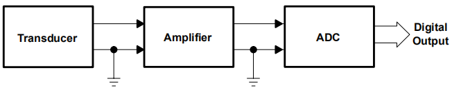
Figure 18–8. Data Acquisition System
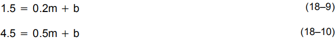
From these equations we find that b = –0.5 and m = 10. The slope and intercept values are substituted into Equation 18–8 to get Equation 8–11.
The mathematical terminology in Equation 18–11 is replaced by electronics terminology in Equation 18–12, and this is the transfer function required for the amplifier. The next step is to select the op amp, and this isn’t a hard task because there are many candidates that could do the job with these undemanding specifications, so let us not dwell on the selection process. Assume that the selected op amp operates on a 5-V power supply, can drive the ADC input resistance of 20 kΩ with no voltage divider action, and that the op amp input impedance is so big that it doesn’t load the transducer.
The circuit that produces the desired transfer function is given in Figure 18–9.

Figure 18–9. Schematic for the Transducer to ADC Interface Circuit
The circuit equation is obtained with the aid of superposition.

Comparing terms between Equations 18–12 and 18–13 enables the extraction of m and b.
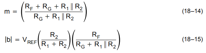
Making the assumption that R1||R2<<RG simplifies the calculations.

Let RG = 20 kΩ, and then RF = 180 kΩ, add, and let VREF = VCC.

Select R2 = 0.82 kΩ and R1 = 72.98 kΩ. Since 72.98 kΩ is not a standard 5% resistor value, R1 is selected as 75 kΩ. The difference between the selected and calculated value of R1 introduces about 3% error in the b coefficient, and this error shows up in the transfer function as an intercept rather than a slope error. The parallel resistance of R1 and R2 is approximately 0.82 kΩ and this is much less than RG which is 20 kΩ, thus the earlier assumption that R1||R2<<RG is justified. R2 could have been selected as a smaller value, but the smaller values yielded poor standard 5% values for R1. The final circuit is shown in Figure 18–10.

Figure 18–10. Final Schematic for the Transducer to ADC Interface Circuit
DAC to Actuator Analog Interface
An amplifier is also used to interface a DAC with an actuator (see Figure 18–11).
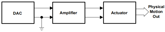
Figure 18–11. Digital Control System
The interface is different from the ADC interface because the DAC output signal is usually current rather than voltage. The first inclination is to stuff the DAC output into a current-to voltage converter like we have always done with split power supplies. This doesn’t always work because the DAC current can be sinked or sourced from ground or the power supply. If a current sourced from the positive power supply is put into a standard current-to-voltage circuit, it wants to drive the op amp output negative, and you need a negative resistor to counter this. The alternate solution for a sourced current from the positive power supply is to terminate the DAC output in a resistor that converts current into voltage, and then
level shift and amplify the terminated voltage. The circuit that performs this function is shown in Figure 18–12.
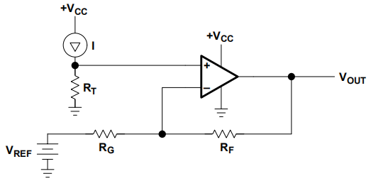
Figure 18–12. DAC Current Source to Actuator Interface Circuit
The DAC output current sources from IOUT(ZEROS) = 1 mA to IOUT(ONES) = 2 mA at an output compliance of 4.33 V. The actuator requires an input voltage swing of VIN1 = 1 V to VIN2 = 4 V to drive it, and its input resistance is 100 kΩ. The system specifications include one 5-V power supply and 5% resistors. The DAC is connected to input of the amplifier (see Figure 18–11), so its output current swing is renamed IIN, and the actuator is connected to the output of the amplifier, so its input voltage range is renamed VOUT. Now, two data points are constructed as IIN1 = 1 mA @ VOUT1 = 1 V and IIN2 = 2 mA @ VOUT2 = 4 V. The data points are substituted into the Equation 18–20. Don’t worry about the sign of m or b because it is determined by the math, and it is substituted into the equation that determines the transfer equation. The simultaneous equations are given below.
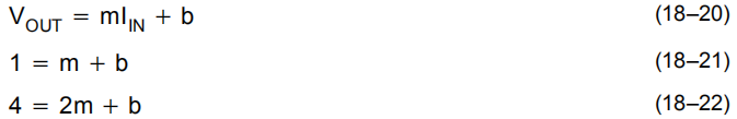
From these equations we find that b = –2 and m = 3. The slope and intercept values are substituted into Equation 18–20 to get Equation 18–23.
The equation for the circuit shown in Figure 18–12 is derived with the aid of superposition, and it is given below in Equation 18–24.

Comparing terms between Equations 18–20 and 18–24 enables the extraction of m and b.

These equations are written in terms of mA and kΩ, so RT = 2.14 kΩ. There is no 2.14-kΩ resistor in the 5% standard values; thus, RT is split into 1.8-kΩ and 0.33-kΩ resistors. RG is selected as 51 kΩ, so RF = 20 kΩ. When IIN = 2 mA VRT = 4.28 V, so the compliance of the DAC is not violated. You might find that standard DACs are not so generous with their compliance specifications.
When the current is sinked from the power supply by the DAC its sign reverses and the previous circuit is not usable. Consider these specifications: the DAC output sinks current from the power supply IOUT(ZEROS) = –1 mA to IOUT(ONES) = –2 mA at an output compliance of 4.33 V. The actuator requires an input voltage swing of VIN1 = 1 V to VIN2 = 4 V to drive it, and its input resistance is 100 kΩ. The system specifications include one 5-V power supply and 5% resistors. The DAC is connected to input of the amplifier (see Figure 18–11), so its output current swing is renamed IIN, and the actuator is connected to the output of the amplifier, so its input voltage range is renamed VOUT. Now, two data points are constructed as IIN1 = –1 mA @ VOUT1 = 1 V and IIN2 = –2 mA @ VOUT2 = 4 V. The data points are substituted into the Equation 18–20. Don’t worry about the sign of m or b because it is determined by the math, and it is substituted into the equation that determines the transfer equation. The transfer function for the current sink DAC is given in Equation 18–29.
The simultaneous equations are given below.
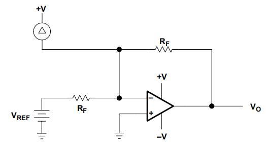
Figure 18–13. DAC Current Sink to Actuator Interface Circuit

From these equations we find that b = –2 and m = –3. The slope and intercept values are substituted into Equation 18–28 to get Equation 18–32.
The current equation for the circuit shown in Figure 18–13 is given below as Equation 18–33, and after algebraic manipulation it becomes Equation 18–34.
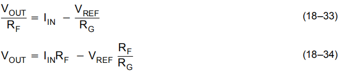
Comparing terms between Equations 18–29 and 18–34 enables the extraction of m and b.

These equations are written in terms of mA and kΩ. RG is selected as 51 kΩ, so RF = 20 kΩ. When IIN = 2 mA, the compliance of the DAC is 0.0 V.
When DAC interface circuits are designed, two parameters that have not been considered in detail can control the design. The DAC has a compliance voltage requirement, and that requirement must be met regardless of the circuit demands. If the DAC compliance requirements are not met, the DAC saturates or is starved for current, and either of these situations introduces considerable error. The actuators driven in these examples are quite benign because most actuators require considerably more current or voltage than is available from an op amp. This fact does not negate the analysis given here. Regardless of the actuator current or voltage requirements, the design procedure is similar. Very often the low voltage device is plugged into a booster that supplies power to the actuator.
One last item to consider is the output capacitance of DACs. The DAC output can have large amounts of stray capacitance that shows up as a capacitor across the op amp inverting input node when the DAC is interfaced into circuits as shown in Figure 18–13. The DAC capacitance from the inverting node to ground acts with RG to form a pole in the op amp loop gain. Adding a pole to the op amp loop gain leads to overshoot, then ringing, and finally oscillation. The effect that the DAC capacitance has on stability must be investigated. Also, the DAC output capacitance is a function of the digital number addressing the DAC. This capacitance can range from near zero to hundreds of pF, thus the op amp must be compensated for the worst case which is the largest capacitance.
Compensation schemes include connecting a capacitor across the feedback resistor. This compensation scheme is called a compensated attenuator, and if the RC time constants are equal, there will excellent performance at that DAC output capacitance. Alas, the circuit can only be ideally compensated at one point, and this point is normally chosen as the highest DAC output capacitance. The remainder of the DAC range suffers from poor bandwidth because of overcompensation.
Comparison of Op Amps
Since the author is only familiar with Texas Instruments op amps, a comparison involving actual op amp parameters would be unfair to other op amp manufacturers. Also, any comparison using today’s production op amps becomes invalid in a short period of time. I write about Texas Instruments op amps, so I get plenty of samples, and the new product introductions come so fast that I have a hard time keeping up with them. The other point to consider is that teaching how to make the op amp comparison is a much more powerful tool, thus a table containing the op amp parameters is established, and each of the parameters is discussed only in terms of low-voltage design.
Table 18–2. Op Amp Parameters

As the table shows, there are a lot of parameters to be considered in the selection of a low voltage op amp. The application weeds out some of these parameters thus easing the selection process. If the application is measuring the output from a low-bandwidth transducer such as a thermocouple, bandwidth is not a parameter of interest, so speed can immediately be sacrificed for power supply current.
When the maximum supply voltage available is 3 V, rafts of op amps requiring more than 3 V operating voltage are eliminated. Taking this concept further, if dynamic range is an important specification in the 3-V design, those op amps that operate on 3 V without RRIO specifications can be eliminated. Because dynamic range is important, the noise voltage and current that detract from dynamic range are important parameters. If this 3-V application requires very low power supply current, the choice is narrowed down to a few candidates. The application selects the op amp, and if this application puts a few more requirements on the 3-V op amp, we may have to design a new IC.
Always start the selection process with the parameter that absolutely can’t be wavered. The next parameter considered in the selection process should be the next most important parameter, and this process is continued parameter by parameter until all requirements are exhausted. Sometimes the supply of op amp candidates runs out before the parameter requirements do. When you reach this point, it is time to renegotiate the design specifications, find a new op amp, negotiate with op amp manufacturers, or announce that you won’t meet specifications. These designs are hard to work because the low power supply voltage requirement and the specifications usually leave very little room to work. As time marches on, more low power supply voltage op amps will come on the market, and these designs will get easier to work.
No comments:
Post a Comment