Operational Amplifier Parameter Glossary
There are usually three main sections of electrical tables in op amp data sheets. The absolute maximum ratings table and the recommended operating conditions table list constraints placed upon the circuit in which the part will be installed. Electrical characteristics tables detail device performance.
Absolute maximum ratings are those limits beyond which the life of individual devices may be impaired and are never to be exceeded in service or testing. Limits, by definition, are maximum ratings, so if double-ended limits are specified, the term will be defined as a range (e.g., operating temperature range). Recommended operating conditions have a similarity to maximum ratings in that operation outside the stated limits could cause unsatisfactory performance. Recommended operating conditions, however, do not carry the implication of device damage if they are exceeded.
Electrical characteristics are measurable electrical properties of a device inherent in its design. They are used to predict the performance of the device as an element of an electrical circuit. The measurements that appear in the electrical characteristics tables are based on the device being operated within the recommended operating conditions. Table 11–1 is a list of parameters and operating conditions that are commonly used in TI op amp data sheets. The glossary is arranged alphabetically by parameter name. An abbreviation cross-reference is provided after the glossary in Table 11–2 to help the designer find information when only an abbreviation is given. More detail is given about important parameters in Section 11.3.
Table 11–1. Op Amp Parameter GLossary


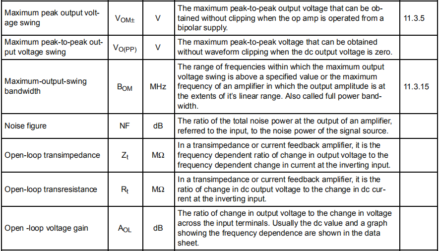


Table 11–2. Cross-Reference of Op Amp Parameters


Input Offset Voltage
All op amps require a small voltage between their inverting and noninverting inputs to balance mismatches due to unavoidable process variations. The required voltage is known as the input offset voltage and is abbreviated VIO. VIO is normally modeled as a voltage source driving the noninverting input.
Figure 11–1 shows two typical methods for measuring input offset voltage — DUT stands for device under test. Test circuit (a) is simple, but since Vout is not at zero volts, it does not really meet the definition of the parameter. Test circuit (b) is referred to as a servo loop. The action of the loop is to maintain the output of the DUT at zero volts. Bipolar input op amps typically offer better offset parameters than JFET or CMOS input op amps.

Figure 11–1.Test Circuits for Input Offset Voltage
TI data sheets show two other parameters related to VIO; the average temperature coefficient of input offset voltage, and the input offset voltage long-term drift. The average temperature coefficient of input offset voltage, αVIO, specifies the expected input offset drift over temperature. Its units are µV/0C. VIO is measured at the temperature extremes of the part, and αVIO is computed as ∆VIO/∆0C.
Normal aging in semiconductors causes changes in the characteristics of devices. The input offset voltage long-term drift specifies how VIO is expected to change with time. Its units are µV/month. VIO is normally attributed to the input differential pair in a voltage feedback amplifier. Different processes provide certain advantages. Bipolar input stages tend to have lower offset voltages than CMOS or JFET input stages. Input offset voltage is of concern anytime that DC accuracy is required of the circuit. One way to null the offset is to use external null inputs on a single op amp package (Figure 11–2). A potentiometer is connected between the null inputs with the adjustable terminal connected to the negative supply through a series resistor. The input offset voltage is nulled by shorting the inputs and adjusting the potentiometer until the output is zero.

Figure 11–2.Offset Voltage Adjust
Input Current
The input circuitry of all op amps requires a certain amount of bias current for proper operation. The input bias current, IIB, is computed as the average of the two inputs:

CMOS and JFET inputs offer much lower input current than standard bipolar inputs. Figure 11–3 shows a typical test circuit for measuring input bias currents. The difference between the bias currents at the inverting and noninverting inputs is called the input offset current, IIO = IN–IP. Offset current is typically an order of magnitude less than bias current.

Figure 11–3.Test Circuit – IIB
Input bias current is of concern when the source impedance is high. If the op amp has high input bias current, it will load the source and a lower than expected voltage is seen. The best solution is to use an op amp with either CMOS or JFET input. The source impedance can also be lowered by using a buffer stage to drive the op amp that has high input bias current.
In the case of bipolar inputs, offset current can be nullified by matching the impedance seen at the inputs. In the case of CMOS or JFET inputs, the offset current is usually not an issue and matching the impedance is not necessary.
The average temperature coefficient of input offset current, αIIO, specifies the expected input offset drift over temperature. Its units are µA/°C. IIO is measured at the temperature extremes of the part, and αIIO is computed as ∆IIO/∆°C.
Input Common Mode Voltage Range
The input common voltage is defined as the average voltage at the inverting and noninverting input pins. If the common mode voltage gets too high or too low, the inputs will shut down and proper operation ceases. The common mode input voltage range, VICR, specifies the range over which normal operation is guaranteed.
Different input structures allow for different input common-mode voltage ranges:
The LM324 and LM358 use bipolar PNP inputs that have their collectors connected to the negative power rail. This allows the common-mode input voltage range to include the negative power rail.
The TL07X and TLE207X type BiFET op amps use P-channel JFET inputs with the sources tied to the positive power rail via a bipolar current source. This allows the common-mode input voltage range to include the positive power rail.
TI LinCMOS op amps use P-channel CMOS inputs with the substrate tied to the positive power rail. This allows the common-mode input voltage range to include the negative power rail.
Rail-to-rail input op amps use complementary N- and P-type devices in the differential inputs. When the common-mode input voltage nears either rail, at least one of the differential inputs is still active, and the common-mode input voltage range includes both power rails.
The trends toward lower, and single supply voltages make VICR of increasing concern.
Rail-to-rail input is required when a noninverting unity gain amplifier is used and the input signal ranges between both power rails. An example of this is the input of an analog-to digital-converter in a low-voltage, single-supply system.
High-side sensing circuits require operation at the positive input rail.
Differential Input Voltage Range
Differential input voltage range is normally specified as an absolute maximum. Exceeding the differential input voltage range can lead to breakdown and part failure. Some devices have protection built into them, and the current into the input needs to be limited. Normally, differential input mode voltage limit is not a design issue.
Maximum Output Voltage Swing
The maximum output voltage, VOM±, is defined as the maximum positive or negative peak output voltage that can be obtained without wave form clipping, when quiescent DC output voltage is zero. VOM± is limited by the output impedance of the amplifier, the saturation voltage of the output transistors, and the power supply voltages. This is shown pictorially in Figure 11–4.

Figure 11–4.VOM
This emitter follower structure cannot drive the output voltage to either rail. Rail-to-rail output op amps use a common emitter (bipolar) or common source (CMOS) output stage. With these structures, the output voltage swing is only limited by the saturation voltage (bipolar) or the on resistance (CMOS) of the output transistors, and the load being driven. Because newer products are focused on single supply operation, more recent data sheets from Texas Instruments use the terminology VOH and VOL to specify the maximum and minimum output voltage.
Maximum and minimum output voltage is usually a design issue when dynamic range is lost if the op amp cannot drive to the rails. This is the case in single supply systems where the op amp is used to drive the input of an A to D converter, which is configured for full scale input voltage between ground and the positive rail.
Large Signal Differential Voltage Amplification
Large signal differential voltage amplification, AVD, is similar to the open loop gain of the amplifier except open loop is usually measured without any load. This parameter is usually measured with an output load. Figure 11–11 shows a typical graph of AVD vs. frequency. AVD is a design issue when precise gain is required. The gain equation of a noninverting amplifier:
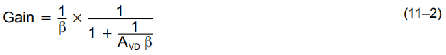
β is a feedback factor, determined by the feedback resistors. The term 1 AVD in the equation is an error term. As long as AVD is large in comparison with 1 , it will not greatly affect the gain of the circuit.
Input Parasitic Elements
Both inputs have parasitic impedance associated with them. Figure 11–5 shows a model of the resistance and capacitance between each input terminal and ground and between the two terminals. There is also parasitic inductance, but the effects are negligible at low frequency.
Input impedance is a design issue when the source impedance is high. The input loads the source.

Figure 11–5.Input Parasitic Elements
Input Capacitance
Input capacitance, Ci , is measured between the input terminals with either input grounded. Ci is usually a few pF. In Figure 11–5, if Vp is grounded, then Ci = Cd || Cn. Sometimes common-mode input capacitance, Cic is specified. In Figure 11–5, if Vp is shorted to Vn, then Cic = Cp || Cn. Cic is the input capacitance a common mode source would see referenced to ground.
Input Resistance
Input resistance, ri is the resistance between the input terminals with either input grounded. In Figure 11–5, if Vp is grounded, then ri = Rd || Rn. ri ranges from 107 Ω to 1012 Ω, depending on the type of input. Sometimes common-mode input resistance, ric, is specified. In Figure 11–5, if Vp is shorted to Vn, then ric = Rp || Rn. ric is the input resistance a common mode source would see referenced to ground.
Output Impedance
Different data sheets list the output impedance under two different conditions. Some data sheets list closed-loop output impedance while others list open-loop output impedance, both designated by Zo.
Zo is defined as the small signal impedance between the output terminal and ground. Data sheet values run from 50 Ω to 200 Ω. Common emitter (bipolar) and common source (CMOS) output stages used in rail-to-rail output op amps have higher output impedance than emitter follower output stages.
Output impedance is a design issue when using rail-to-rail output op amps to drive heavy loads. If the load is mainly resistive, the output impedance will limit how close to the rails the output can go. If the load is capacitive, the extra phase shift will erode phase margin. Figure 11–6 shows how output impedance affects the output signal assuming Zo is mostly resistive.

Figure 11–6.Effect of Output Impedance
Some new audio op amps are designed to drive the load of a speaker or headphone directly. They can be an economical method of obtaining very low output impedance.
Common-Mode Rejection Ratio
Common-mode rejection ratio, CMRR, is defined as the ratio of the differential voltage amplification to the common-mode voltage amplification, ADIF/ACOM. Ideally this ratio would be infinite with common mode voltages being totally rejected.
The common-mode input voltage affects the bias point of the input differential pair. Because of the inherent mismatches in the input circuitry, changing the bias point changes the offset voltage, which, in turn, changes the output voltage. The real mechanism at work is ∆VOS/∆VCOM.
In a Texas Instruments data sheet, CMRR = ∆VCOM/∆VOS, which gives a positive number in dB. CMRR, as published in the data sheet, is a dc parameter. CMRR, when graphed vs. frequency, falls off as the frequency increases. A common source of common-mode interference voltage is 50-Hz or 60-Hz ac noise.
Care must be used to ensure that the CMRR of the op amp is not degraded by other circuit components. High values of resistance make the circuit vulnerable to common mode (and other) noise pick up. It is usually possible to scale resistors down and capacitors up to preserve circuit response.
Supply Voltage Rejection Ratio
Supply voltage rejection ratio, kSVR (AKA power supply rejection ratio, PSRR), is the ratio of power supply voltage change to output voltage change. The power voltage affects the bias point of the input differential pair. Because of the inherent mismatches in the input circuitry, changing the bias point changes the offset voltage, which, in turn, changes the output voltage.
For a dual supply op amp,

The term ∆VCC± means that the plus and minus power supplies are changed symmetrically. For a single supply op amp,

Also note that the mechanism that produces kSVR is the same as for CMRR. Therefore kSVR as published in the data sheet is a dc parameter like CMRR. When kSVR is graphed vs. frequency, it falls off as the frequency increases.
Switching power supplies produce noise frequencies from 50 kHz to 500 kHz and higher. kSVR is almost zero at these frequencies so that noise on the power supply results in noise on the output of the op amp. Proper bypassing techniques must be used (see Chapter 17) to control high-frequency noise on the power lines.
Supply Current
Supply current, IDD, is the quiescent current draw of the op amp(s) with no load. In a Texas Instruments data sheet, this parameter is usually the total quiescent current draw for the whole package. There are exceptions, however, such as data sheets that cover single and multiple packaged op amps of the same type. In these cases, IDD is the quiescent current draw for each amplifier.
In op amps, power consumption is traded for noise and speed.
Slew Rate at Unity Gain
Slew rate, SR, is the rate of change in the output voltage caused by a step input. Its units are V/µs or V/ms. Figure 11–7 shows slew rate graphically. The primary factor controlling slew rate in most amps is an internal compensation capacitor CC, which is added to make the op amp unity gain stable. Referring to Figure 11–8, voltage change in the second stage is limited by the charging and discharging of the compensation capacitor CC. The maximum rate of change is when either side of the differential pair is conducting 2IE. Essentially SR = 2IE/CC. Remember, however, that not all op amps have compensation capacitors. In op amps without internal compensation capacitors, the slew rate is determined by internal op amp parasitic capacitances. Noncompensated op amps have greater bandwidth and slew rate, but the designer must ensure the stability of the circuit by other means. In op amps, power consumption is traded for noise and speed. In order to increase slew rate, the bias currents within the op amp are increased.

Figure 11–7.Figure 6. Slew Rate

Figure 11–8.Figure 7. Simplified Op Amp Schematic
Equivalent Input Noise
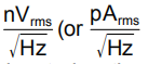
All op amps have parasitic internal noise sources. Noise is measured at the output of an op amp, and referenced back to the input. Therefore, it is called equivalent input noise. Equivalent input noise parameters are usually specified as voltage, Vn, (or current, In) per root Hertz. For audio frequency op amps, a graph is usually included to show the noise over the audio band.
Spot Noise
The spectral density of noise in op amps has a pink and a white noise component. Pink noise is inversely proportional to frequency and is usually only significant at low frequencies. White noise is spectrally flat. Figure 11–9 shows a typical graph of op amp equivalent input noise.
Usually spot noise is specified at two frequencies. The first frequency is usually 10 Hz where the noise exhibits a 1/f spectral density. The second frequency is typically 1 kHz where the noise is spectrally flat. The units used are normally
for current noise). In Figure 11–9 the transition between 1/f and white is denoted as the corner frequency, fnc.
Broadband Noise
A noise parameter like VN(PP), is the a peak to peak voltage over a specific frequency band, typically 0.1 Hz to 1 Hz, or 0.1 Hz to 10 Hz. The units of measurement are typically nV P–P.
Given the same structure within an op amp, increasing bias currents lowers noise (and increases SR, GBW, and power dissipation).
Also the resistance seen at the input to an op amp adds noise. Balancing the input resistance on the noninverting input to that seen at the inverting input, while helping with offsets due to input bias current, adds noise to the circuit.

Figure 11–9.Typical Op amp Input Noise Spectrum
Total Harmonic Distortion Plus Noise
Total harmonic distortion plus noise, THD + N, compares the frequency content of the output signal to the frequency content of the input. Ideally, if the input signal is a pure sine wave, the output signal is a pure sine wave. Due to nonlinearity and noise sources within the op amp, the output is never pure.
THD + N is the ratio of all other frequency components to the fundamental and is usually specified as a percentage:

Figure 11–10 shows a hypothetical graph where THD + N = 1%. The fundamental is the same frequency as the input signal. Nonlinear behavior of the op amp results in harmonics of the fundamental being produced in the output. The noise in the output is mainly due to the input noise of the op amp. All the harmonics and noise added together make up 1% of the fundamental.
Two major reasons for distortion in an op amp are the limit on output voltage swing and slew rate. Typically an op amp must be operated at or below its recommended operating conditions to realize low THD.

Figure 11–10. Output Spectrum with THD + N = 1%
Unity Gain Bandwidth and Phase Margin
There are five parameters relating to the frequency characteristics of the op amp that are likely to be encountered in Texas Instruments data sheets. These are unity-gain bandwidth (B1), gain bandwidth product (GBW), phase margin at unity gain (φm), gain margin (Am), and maximum output-swing bandwidth (BOM).
Unity-gain bandwidth (B1) and gain bandwidth product (GBW) are very similar. B1 specifies the frequency at which AVD of the op amp is 1:
GBW specifies the gain-bandwidth product of the op amp in an open loop configuration and the output loaded:
GBW is constant for voltage-feedback amplifiers. It does not have much meaning for current-feedback amplifiers because there is not a linear relationship between gain and bandwidth.
Phase margin at unity gain (φm) is the difference between the amount of phase shift a signal experiences through the op amp at unity gain and 180:
Gain margin is the difference between unity gain and the gain at 180 phase shift:
Maximum output-swing bandwidth (BOM) specifies the bandwidth over which the output is above a specified value:
The limiting factor for BOM is slew rate. As the frequency gets higher and higher the output becomes slew rate limited and can not respond quickly enough to maintain the specified output voltage swing.
In order to make the op amp stable, capacitor, CC, is purposely fabricated on chip in the second stage (Figure 11–8). This type of frequency compensation is termed dominant pole compensation. The idea is to cause the open-loop gain of the op amp to roll off to unity before the output phase shifts by 180. Remember that Figure 11–8 is very simplified, and there are other frequency shaping elements within a real op amp.
Figure 11–11 shows a typical gain vs. frequency plot for an internally compensated op amp as normally presented in a Texas Instruments data sheet. As noted earlier, AVD falls off with frequency. AVD (and thus B1 or GBW) is a design issue when precise gain is required of a specific frequency band.
Phase margin (φm) and gain margin (Am) are different ways of specifying the stability of the circuit. Since rail-to-rail output op amps have higher output impedance, a significant phase shift is seen when driving capacitive loads. This extra phase shift erodes the phase margin, and for this reason most CMOS op amps with rail-to-rail outputs have limited ability to drive capacitive loads.

Figure 11–11.Voltage Amplification and Phase Shift vs. Frequency
Settling Time
It takes a finite time for a signal to propagate through the internal circuitry of an op amp. Therefore, it takes a period of time for the output to react to a step change in the input. In addition, the output normally overshoots the target value, experiences damped oscillation, and settles to a final value. Settling time, ts, is the time required for the output voltage to settle to within a specified percentage of the final value given a step input.

Figure 11–12. Settling Time
Settling time is a design issue in data acquisition circuits when signals are changing rapidly. An example is when using an op amp following a multiplexer to buffer the input to an A to D converter. Step changes can occur at the input to the op amp when the multiplexer changes channels. The output of the op amp must settle to within a certain tolerance before the A to D converter samples the signal.
No comments:
Post a Comment