Wireless Systems
High-speed operational amplifiers (op amps) are used extensively in wireless communication systems. These amplifiers typically operate at intermediate frequencies (IF) ≤ 500 MHz and most frequently operate below 25 MHz. Applications for high-speed op amps include filtering circuits in radio receivers, IF amplifiers, mixer circuits, and bandpass amplifiers.
This chapter focuses on the requirements for the op amp and a number of techniques used in wireless communication systems to interface high-speed op amps to analog-to digital converters (ADCs) and digital-to-analog converters (DACs). This section provides several examples of different op amp usage.
Figure 13–1 shows an example of a dual-IF receiver. In this application, several stages with different IF frequencies are used to get the desired performance. The receiver converts the received radio frequency (RF) input from the antenna to a baseband signal. This type of system requires the ability to receive and operate over a wide range of signal strength. The inherent system noise level determines the lower operating limit and is a critical factor in the overall performance of the receiver. The receiver performance is measured in terms of receiver sensitivity, which is defined as the ratio between the power of the wanted baseband signal at the output of the ADC and the total power of all unwanted signals (include random noise, aliasing, distortion, and phase noise contributed by the local oscillator) introduced by the different circuit elements in the receiver. A low-sensitivity receiver can cause signal saturation in the ADC input.

Figure 13–1. A Typical GSM Cellular Base Station Receiver Block Diagram
The receiver contains two mixer stages reminiscent of a classic superhetrodyne receiver with good selectivity. The process of hetrodyning involves the translation of one frequency to another by the use of a mixer and local oscillator (LO) offset at the proper frequency to convert the RF signal to the desired IF. The LO signal is at a much higher level than the RF signal. In Figure 13–1, the 900 MHz RF signal is picked up by the antenna and amplified by a low-noise amplifier (LNA). After being sufficiently amplified by the LNA to overcome the noise level, the RF signal passes through a bandpass filter (BPF) used to provide image rejection and sufficient selectivity prior to the first stage mixing.
High selectivity prevents adjacent channel energy from getting into the input of the ADC and decreasing the receiver dynamic range. A strong signal in an adjacent channel causes intermodulation products in the receiver that can result in loss of the received signal. The band-pass filter is implemented with a surface acoustic wave (SAW) filter. The SAW filter provides very sharp edges to the passband, with minimum ripple and phase distortion.
The first stage mixer down-converts the band-limited RF signal with the LO signal, producing a number of new frequencies in the spectrum, including the sum frequency component, the difference frequency component, and spurious responses. The first stage IF filter provides sufficient filtering after the mixing circuit. It selects the difference frequency component while rejecting the sum frequency component and undesirable spurious responses. Passing the difference frequency component on to the next stage of the receiver makes it much easier to provide the gain and filtering needed for proper receiver functionality. Image rejection also places a constraint on the choice of the IF (10 MHz – 20 MHz). The spurious responses are the result of power supply harmonics and intermodulation products created during the mixing of the RF signal and the LO signal. If not substantially suppressed, spurious responses often corrupt the IF signal and cause it to be accepted as a valid IF signal by the IF amplifier.
The first stage IF amplifier minimizes the effects of the first stage filter loss on the noise figure and amplifies the signal to a suitable level for the second stage mixer. The output from the second stage mixer is applied to the second stage IF amplifier, automatic gain control (AGC) amplifier, and the subsequent low-pass filter, producing a 1-V full-scale input to the ADC. The ADC samples and digitizes this baseband analog input. The AGC amplifier ensures that if the received signal amplitude goes up rapidly, the ADC is not saturated. At the other extreme, if there is a fast power ramp down, the AGC prevents the signal quality from passing below an acceptable level. High-speed current-feedback operational amplifiers (CFA) are typically used to filter and amplify the IF signals because this type of operational amplifier has good slew rate, wide bandwidth, large dynamic range, and a low noise figure.
In this type of receiver, the ADC is a key component requiring sampling rates ≥ 40 MSPS with 12 bits to 14 bits of resolution and is usually a pipeline architecture device. The output of the ADC is highly dependent on the ADC’s sampling frequency, nonlinearities in the ADC and the analog input signal, and the converter maximum frequency.
Table 13–1 tabulates the contribution of each stage depicted in Figure 13–1 to the system level budget for a typical GSM receiver. GSM is the global system for mobile communications. It is one of the most popular digital cellular formats in the world.
Table 13–1. GSM Receiver Block System Budget
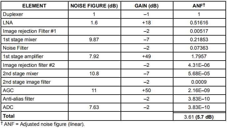
Figure 13–2 shows a more flexible implementation for the receiver using a digital signal processor (DSP). Using a DSP allows a single receiver to access several different wireless systems through changes in software configuration.

Figure 13–2. An Implementation of a Software-Configurable Dual-IF Receiver
Figure 13–3 shows a basic W-CDMA transmit chain. A voiceband CODEC (coder–decoder), op amps, and a DSP are used to digitize and band-limit the audio signal. The digitized signal is then compressed to the appropriate data rate either in hardware or by a software program implemented on the DSP. Redundancy (error correction), encryption, and the appropriate form of modulation (QPSK for W–CDMA or GMSK for GSM) are added to the compressed digitized signal. This signal goes via an interpolating filter to the communication DAC as shown in Figure 13–4. Eight times interpolation[1],[2] is shown in Figure 13–4, but other multiple-of-2 interpolations are possible and quite often used. Assuming that the modulated bit stream is a 3.84 MSPS W–CDMA signal, for 8x interpolation, the sampling clock frequency would need to be 30.72 MHz. The DAC converts the modulated bit stream to analog, and the conversion is usually performed by a pair of DACs: one for I channel and one for Q channel — see Figure 13–3. The reconstruction filter, at the output of the DAC, is usually a high-order Bessel or elliptic filter used to low-pass filter the analog output from the DAC.

Figure 13–3. Basic W-CDMA Cellular Base Station Transmitter Block
The modulator block converts the baseband I and Q signal to the appropriate carrier frequency, typically 864 MHz. The up-converted 864 MHz signal is amplified to a suitable level by the power amplifier (PA) and sent out via the antenna over the air or to a nearby wireless base station.
The RF power amplifier is a large-signal device with power gain and efficiency on the order of 50% for GSM and about 30% for code division multiple access (CDMA), an access method in which multiple users are permitted simultaneously on the same frequency.

Figure 13–4. Communication DAC with Interpolation and Reconstruction Filters
Selection of ADCs/DACs
In communication applications, the dc nonlinearity specifications that describe the converter’s static performance are less important than the dynamic performance of the ADC. The receiver (overall system) specifications depend very much on the ADC dynamic performance parameters: effective number of bits (ENOB), SFDR (spurious free dynamic range), THD (total harmonic distortion), and SNR (signal-to-noise ratio). Good dynamic performance and fast sampling rate are required for accurate conversion of the baseband analog signal at RF or IF frequencies. The SFDR specification describes the converter’s in-band harmonic characterization and it represents the converter’s dynamic range. SFDR is slew rate and converter input frequency dependent.
The output from an ADC is highly dependent on the converter sampling frequency and the maximum frequency of the analog input signal. A low-pass or band-pass anti-aliasing filter placed immediately before the ADC band-limits the analog input. Band-limiting ensures that the original input signal can be reconstructed exactly from the ADC’s output samples when a sampling frequency (ƒs) of twice the information bandwidth of the analog input signal is used (Nyquist sampling). Undesirable signals, above ƒs/2, of a sufficient level, can create spectrum overlap and add distortion to the desired baseband signal. This must not be allowed to dominate the distortion caused by ADC nonlinearities. Sampling at the Nyquist rate places stringent requirements on the anti-aliasing filter — usually a steep transition 10th or higher order filter is needed.
Oversampling techniques (sampling rate greater than the Nyquist rate) can be employed to drastically reduced the steepness of the anti-aliasing filter rolloff and simplify the filter design. However, whenever oversampling is used, a faster ADC is required to digitize the input signal. Very fast ADCs can be costly and they consume a fair amount of power (≥ 1000 mW). In a system application, such as a wireless base station, where large numbers of ADCs are used, the individual device power consumption must be kept to the bare minimum (≤ 400 mW). High-resolution ADCs, with slower sampling rates, offer potential cost savings, lower power consumption, and good performance, and are often used in some applications. In this case, undersampling or bandpass sampling techniques (the analog signal digitization by the ADC exceeds half the sampling frequency (ƒs) of the ADC, but the signal information bandwidth is ≤ ƒs/2) are employed.
Operating the ADC in a bandpass sampling application requires knowledge of the converter’s dynamic performance for frequencies above ƒs/2. In general, as the input signal frequency to the converter increases, ENOB, SNR, SFDR, and harmonic performance degrades.
The fact that the analog input to the ADC cannot be represented exactly with a limited number of discrete amplitude levels introduces quantization error into the output digital samples. This error is given by the rms quantization error voltage
The mean squared quantization noise power is

where qs is the quantization step size and R is the ADC input resistance, typically 600 Ω to 1000 Ω.
Communication ADCs similar to the THS1052 and THS1265 typically have a full scale range (FSR) of 1 Vp–pto 2 Vp–p. Generally, wireless systems are based on a 50-Ω input/output termination, therefore, the ADC input is made to look like 50 Ω. Based on this assumption, the quantization noise power for a 12-bit, 65 MSPS ADC (THS1265) is –73.04 dBm.
For a noise-limited receiver, the receiver noise power can be computed as the thermal noise power in the given receiver bandwidth plus the receiver noise figure NF[3].
For 200 kHz BW (GSM channel), temperature 25C, and 4 dB to 6 dB NF, the receiver noise power is –115 dBm. Therefore, to boost the receiver noise to the quantization noise power level requires a gain of 42 dB.
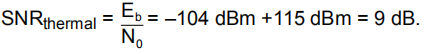
In Figure 13–1, the GSM–900 signal is at –104 dBm (GSM–900 spec for smallest possible signal at which the raw bit-error rate must meet or exceed 1%) and, therefore, the signal to-noise ratio (SNR) at baseband or at the converter and due to the thermal noise component is given by
In order for the raw BER to be 1% in a GSM system, testing and standard curves [4] indicate, that a baseband SNR (derived from the sum of both thermal noise and ADC noise) of 9 dB is needed for this performance node.
The process gain Gp is defined as:

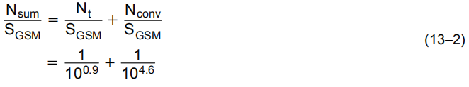
where GSM channel BW = 200 kHz and ƒs = 52 MHz (the ADC sampling frequency). The converter noise at baseband should be much better than the radio noise ( = thermal noise + process gain). Furthermore, the thermal noise alone brings the system only to the reference bit-error rate (BER).
Therefore the converter noise (at baseband) = SNRadc + process gain Gp.
The ADC SNRadc should be 20 dB to 40 dB above the SNRthermal of the thermal noise component (+9 dBm). In this example, ADC SNRadc is selected to be 37 dB better than the SNRthermal of the thermal noise component (9 dB).
In other words, if the converter SNRadc is desired to be 37 dB better than the thermal noise component (SNRthermal), the baseband converter is chosen to be 9 + 37 dB = 46 dB. The total noise (Nsum) = thermal noise (Nt) + converter noise (Nconv).
Therefore, the noise-to-signal ratio is:
The signal-to-noise ratio
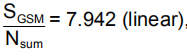
which is 8.999 dB.
This shows that the converter noise degenerates the baseband SNR due to thermal noise alone, by only 0.0001 dB (9.000 dBm – 8.999 dB) when the signal is at reference sensitivity level. At fs = 52 MSPS, the converter SNRadc required to fit the GSM–900 signal is (46 – 24.15) dB = 22 dB.
The effective number of bits (ENOB) required for fitting the GSM–900 signal is

and thus 4 bits are needed for the GSM–900 signal.
Assuming that filter #3 attenuates the interferer by 50 dB, the interferer drops from –13 dBm to –53 dBm, or 40 dB above the GSM signal. The requirements for the number of bits needed to accommodate the interferer is
Approximately 6 bits are needed to accommodate the interferer, plus 2 bits of head room for constructive interference, for a total of 8 bits. The ADC requirements are 4 bits for the GSM signal plus 8 bits for the interferer for a total of 12 bits:
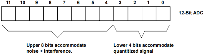
It follows from the above analysis that the GSM signal is 8 bits down, or 8 bits x 6 dB/bit = 48 dB down from the 1 V FSR of the ADC. The full-scale input power to an ADC having a 50-Ω termination can be calculated as:

Therefore, the 4 bits for the GSM signal gives 13 dBm – (8 bits x 6 dB/bit) = –35 dBm, the smallest possible ADC input signal power with the interferer that will meet the GSM specification. Without the interferer present, the signal level is chosen to be about 20 dB below the ADC full scale, or –8 dBm, to accommodate constructive interference and to accommodate any large ADC input signal that may arise from short-term errant gain due to gain settling in the AGC. Thus, with the smallest possible signal specified by the GSM–900 spec, the signal is amplified from –104 dBm to –8dBm without the interferer, and to –35 dBm with the interferer.
For a practical receiver, as shown in Figure 13–1, an AGC is necessary to assure that the LSB represents a uniform noise input while the peak power does not exceed the ADC’s FSR.
The receiver block shown in Figure 13–1 uses a high-speed, fairly wide bandwidth (100 MHz to 550 MHz) communication ADC to convert the baseband signal to a high speed parallel bit stream for processing in a DSP. For an ADC to accurately produce a digital version of the baseband analog input, the device must have very good resolution and dynamic performance.
The signal path shown in Figure 13–1 needs 95 dB of gain in order to bring the –104 dBm GSM signal up to –9 dBm (equivalent to about 0.112 Vp–p across 50 Ω), with allowances for losses in the filters, and mixers. Usually this gain is split evenly between the RF and baseband, but baseband gain is less expensive and consumes less power. The LNA provides 18 dB, which, after filtering and cable losses, yields about 16 dB, while the mixer provides –7 dB of conversion gain/loss.
Modern communication DACs are, effectively, an array of matched current sources optimized for frequency domain performance. To handle both strong and weak signals, communication DACs require large dynamic range. The dynamic specifications of most interest are SFDR, SNR, THD, IMD (two-tone intermodulation distortion), ACPR (adjacent channel power rejection), and settling time.
Besides these, there are a number of dc parameters, such as integral nonlinearity (INL) and differential nonlinearity (DNL), that are considered important because of their influence on the SFDR parameter. DNL errors occur only at certain points in the converter’s transfer function. INL and DNL errors appear as spurious components in the output spectrum and can degrade the signal-to-noise ratio of the DAC.
Typical SFDR figures for 12-bit DACs and 14-bit DACs, with a 5-MHz single tone input at 50 MSPS, range from 75 dB to 80 dB. In order to prevent adjacent communication channels from interfering with each other, the DAC must exhibit a good SFDR specification. Communication DACs normally have differential outputs, and the current-mode architecture is used to give the DAC a higher update rate.
Factors Influencing the Choice of Op Amps
IF amplifiers and filters can be built from discrete components, though most modern applications use integrated circuits. High-speed wideband op amps are employed as buffer amplifiers in the LO circuit, at the front end of ADCs, at the output of the DAC, in the external voltage reference circuits for ADCs and DACs, and in the AGC amplifier and anti-aliasing stage. Op amps operating at IF frequencies, such as the AGC amplifier in Figure 13–1, must attain a large gain control range. How well the amplifier handles large and small signals is a measure of its dynamic range. The current-feedback op amp can be used everywhere except for the anti-aliasing filter and in the reconstruction filter stage. The op amp must have a level gain response from almost dc to at least 500 MHz, after which a gentle rolloff is acceptable. Also, the phase response is important to avoid dispersing the signal — this requires a linear phase response.
Several factors influence the choice of the current-feedback op amp (CFA) and voltagefeedback amplifier (VFA) for use in wireless communication systems:
The ADC/DAC resolution
ADC/DAC dynamic specification
Operating frequencies
Type of signal
Supply voltages and
Cost
In both the receiver and transmit circuits, shown in Figures 13–1 and 13–3, the SFDR and IMD are the key ADC/DAC parameters that have the most influence on op amp selection. A minimum requirement is that the op amp’s SFDR or THD parameter, measured at the frequency of operation, should be 5 dB to 10 dB better than the converter’s SFDR. For a perfect 12-bit ADC, the SFDR is 72 dB, thus the op amp in front of the ADC should exhibit a SFDR (or THD) of 77 dB to 82 dB.
When an op amp is used as a buffer amplifier, it must faithfully reproduce the input to a very high degree of accuracy. This requires that the amplifier be designed and optimized for settling time. Fast settling time is mandatory when driving the analog input of an ADC because the op amp output must settle to within 1 LSB of its final value (within a time period set by the sampling rate) before the ADC can accurately digitize the analog input. The amplifier settling time determines the maximum data transfer rate for a given accuracy. For example, to settle within 1 LSB of full scale range implies that the settling accuracy of the ADC is ± LSB. Hence, a 12-bit ADC will require the op amp to settle to
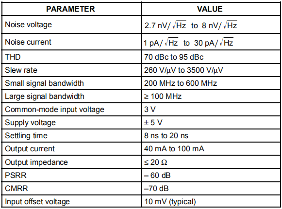
of final value, or 0.0122% of final value. An LSB = 244 µV for a 12-bit ADC with 1 V full-scale range. Values for the settling time and other important op amp parameters as they relate to the receiver and transmit blocks are listed in Table 13–2.
The op amp dynamic parameters in Table 13–2 represent the range of values to achieve low noise, good SFDR, high slew rate, good bandwidth, etc.
Table 13–2. High-Speed Op Amp Requirements
Op amps operating from ± 5-V supplies typically have 6 V to 8 V of common-mode range. Single-supply op amps often handle much smaller voltage ranges, and in some communication applications, could exhibit limited linear operation over a wide signal swing. With the exception of rail-to-rail op amps, most op amps can swing to within 1 V to 1.5 V of the positive rail. Typically signal-to-noise ratio, slew rate, and bandwidth suffer for devices operating from low supply voltages.
When selecting current-feedback op amps, the gain-bandwidth plots are essential. They are needed because with current feedback ordinary loop-gain-proportional bandwidth relationships do not hold.
Anti-Aliasing Filters
Spurious effects in the receiver channel (Figure 13–1) appear as high frequency noise in the baseband signal present at the ADC. The spurious signals (> ƒs/ 2) must be blocked from getting to the ADC (sampling at Nyquist rate, ƒs) where they will cause aliasing errors in the ADC output.
A suitable anti-aliasing low-pass analog filter placed immediately before the ADC can block all frequency components capable of causing aliasing from reaching the ADC. The anti-aliasing filter cutoff frequency (fc) is set to the highest baseband signal frequency of interest (fmax) so that fc = fmax. Sampling theorem requires that the ADC minimum Nyquist rate sampling frequency fs = 2fmax. This ensures that the original base band or IF signal can be reconstructed exactly from the ADC’s digital outputs. It is important to know that only an anti-aliasing filter having a brickwall-type response could fully satisfy the exacting requirements imposed by the sampling theorem. The rolloff of real filters increases more gradually from cutoff to the stop band, and therefore, in practice, the ADC sampling frequency is usually slightly higher than 2ƒmax.
The anti-aliasing filter must reduce the out-of-band aliasing producing signals to less than 1 LSB of the ADC resolution, without introducing additional distortion of the baseband or IF signal in-band components and without predominating distortion due to the ADC nonlinearities. The spectrum overlap (aliasing) requirements are determined by:
Highest frequency of interest
Sampling rate
ADC resolution
The highest signal frequency of interest sets the filter cutoff frequency. For example, suppose the input signal is to be sampled to 12-bit accuracy with a sampling frequency of 52 MHz. If the IF signal is 17 MHz an 18 MHz filter –3dB cutoff frequency could be chosen.
All frequencies above the Nyquist frequency should be attenuated to ≤ LSB, but generally only frequencies above the ADC’s limit of resolution will be a problem; i.e., ƒalias = (52 – 17) MHz = 35 MHz. The frequency rolloff is 18 MHz to 35 MHz (about 1 octave) and the required attenuation is 72 dB (12-bit ADC). A very high-order filter is required to accomplish this task. Practical ant-aliasing filters are limited to fifth-order or sixth-order type because of amplifier bandwidth, phase margin, layout parasitics, supply voltage, and component tolerances. Keep in mind that as the rolloff sharpens, the passband ripple and phase distortion increase.
For communication applications, linear phase characteristic and gain accuracy (low passband ripple) are important. And normally, Chebychev or elliptic (Cauer) filter types are used for the anti-aliasing filter.
For good transient response or to preserve a high degree of phase coherence in complex signals, the filter must be of linear-phase type (Bessel-type filter). The THS4011 or THS4021 voltage-feedback op amp is a good choice for implementing anti-aliasing filter in this example.
The quality of the capacitors and resistors used to implement the design is critical for performance anti-aliasing filter.
Communication D/A Converter Reconstruction Filter
Modern communication DACs are, effectively, an array of matched current sources optimized for frequency domain performance. The most important dynamic specifications are SFDR, SNR, THD, IMD, ACPR and settling time. The dc parameters INL and DNL are considered important because of their influence on the SFDR parameter. Typical SFDR figures for 12-bit to 14-bit DACs, with a 5-MHz single-tone input at 50 MSPS, ranges from 75 dB to 80 dB. In order to prevent adjacent communication channels from interfering with each other, the DAC must exhibit a good SFDR specification.
Communication DACs normally have differential outputs and current-mode architecture is used to give the DAC a higher update rate.
Figure 13–4 shows an interpolating filter block before the DAC and the reconstruction analog filter at the output of the DAC. The interpolating filter is a digital filter whose system clock frequency is an integer multiple of the filter input data stream and is employed to reduce the DAC’s in-band aliased images. This eases the job of the reconstruction filter at the output of the DAC. The filter is used to smooth the input data — the output waveform frequency is the same as the input to the interpolating filter. Figure 13–5 shows the interpolation filter output. The system clock frequency of the DAC and the interpolating filter are running at the same rate; therefore, the frequency spectrum of the DAC output signal, repeated at integer multiples of the sampling rate, becomes increasingly separated as the sampling rate is increased. The further apart the repeated DAC output spectrum, then the less steep the attenuation characteristic of the anti-aliasing needs to be. Consequently, a simpler anti-aliasing filter with a less steep rolloff from pass band to stop band can be used without any increase in distortion due to aliasing. In Figure 13–4, the system clock is 30.772 MHz (3.84 MSPS x 8). Figure 13–6 shows the attenuation characteristics needed for the reconstruction anti-aliasing filter.
The aliasing frequency is ƒalias = (28.7 – 2) = 26.7 MHz, and the required attenuation is 84 dB (14-bit DAC). A third-order anti-aliasing low-pass elliptic or Bessel filter could be used to meet the attenuation requirements. Either type of high-order filter gives a relatively flat response up to just below the sampling frequency, followed by a sharp cutoff. But this arrangement provides no correction for the sinc function (Sinx)/x falloff in amplitude naturally produced by the sample and hold function in the DAC.
The tradeoff in building a simpler reconstruction filter is that a faster DAC is required to convert the input digital data stream to analog signal.

Figure 13–5. QPSK Power Spectral Density Without Raised Cosine Filter — W-CDMA

Figure 13–6. Reconstruction Filter Characteristics
Figure 13–7 shows a first-order reconstruction (low-pass) filter consisting of a high-speed differential amplifier configured for unity gain. The DAC outputs are terminated into 50 Ω. In Figure 13–7, the value for the filter capacitor is given by the expression:


Figure 13–7. A Single-Pole Reconstruction Filter
External Vref Circuits for ADCs/DACs
Figure 13–8 shows an op amp voltage follower circuit that is often used to interface the external precision voltage reference supplying the ADC/DAC external reference voltage (see for example, Miller and Moore, [5], [6],1999, 2000 for a more detailed discussion on voltage reference circuits used in ADC an DAC systems). Vin is the output from a precision voltage reference, such as the Thaler Corp. VRE3050. The low-pass filter (formed by C1R1) filters noise from the reference and op amp buffer. The –3 dB corner frequency of the filter is 1/2πC1R1and the transfer function for this circuit can be written as

which has a zero at s = C2R2.
With the approximation C2R2 = 2C1R1, the denominator polynomial is solved for complex poles p1 and p2 of the response, which results in:


Figure 13–8. Voltage Reference Filter Circuit
The zero in the numerator of the transfer function improves the relative stability of the circuit. Resistor R2 should be kept fairly low, since a small amount of bias current flows through it and causes dc error and noise. Resistor R1 value ranges from 10 Ω to 50 Ω.
Resistor R1 is in the feedback loop, so any small leakage current that is due to capacitor C1 flows through R1and the voltage dropped across R1 is divided by the loop gain. For all practical purposes, the voltage across C2 is 0 V and hence give rise to negligible leakage current.
A design example for a 3-kHz bandwidth filter is illustrated:
Choose C1 = 1.2 µF and R1 = 42.2 Ω.
Having determined the value for C1 and R1, the capacitor C2 value is estimated to be approximately 4% to 5% of C1 value (C2 = 0.047 µF) and resistor R2 is calculated using the approximation C2R2 = 2C1R1 (R2 = 2.15 kΩ).
The calculated –3-dB bandwidth for the circuit is 3.1 kHz and this value agrees with the circuit’s frequency response plot shown in Figure 13–9. This circuit topology is good for driving large capacitive loads.
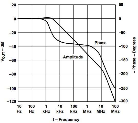
Figure 13–9. Voltage Follower Frequency Response Plot
Figure 13–10 shows an external reference circuit that provides a wide adjustment range of the ADC full-scale range. Resistors R281 and R282 play two roles in this circuit:
Form part of the low-pass filter used to rolloff noise
Isolate the ADC’s reference input load capacitance from the buffer op amp output
Potentiometer R247 sets the external common-mode voltage (Vocm) for the differential amplifier in Figure 13–11.
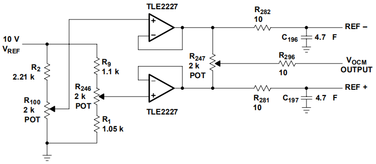
Figure 13–10. External Voltage Reference Circuit for ADC/DAC.
High-Speed Analog Input Drive Circuits
Communication ADCs, for the most part, have differential inputs and require differential input signals to properly drive the device. Drive circuits are implemented with either RF transformers or high-speed differential amplifiers with large bandwidth, fast settling time, low output impedance, good output drive capabilities, and a slew rate of the order of 1500 V/µS. The differential amplifier is usually configured for a gain of 1 or 2 and is used primarily for buffering and converting the single-ended incoming analog signal to differential outputs. Unwanted common-mode signals, such as hum, noise, dc, and harmonic voltages are generally attenuated or cancelled out. Gain is restricted to wanted differential signals, which are often 1 V to 2 V.
The analog input drive circuit, as shown in Figure 13–11, employs a complementary bipolar (BiCom) THS4141 device. BiCom offers fast speed, linear operation over a wide frequency range, and wide power-supply voltage range, but draws slightly more current than a BiCMOS device. The circuit closed-loop response is shown in Figure 13–12, where the –3-dB bandwidth is 120 MHz measured at the output of the amplifier. The analog input Vin is ac-coupled to the THS4141 and the dc voltage Vocm is the applied input common mode voltage. The combination R47– C57 and R26 – C34 are selected to meet the desired frequency rolloff. If the input signal frequency is above 5 MHz, higher-order low-pass filtering techniques (third-order or greater) are employed to reduce the op amp’s inherent second harmonic distortion component.
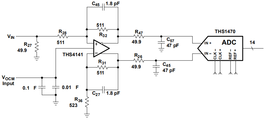
Figure 13–11. Single-Ended to Differential Output Drive Circuit
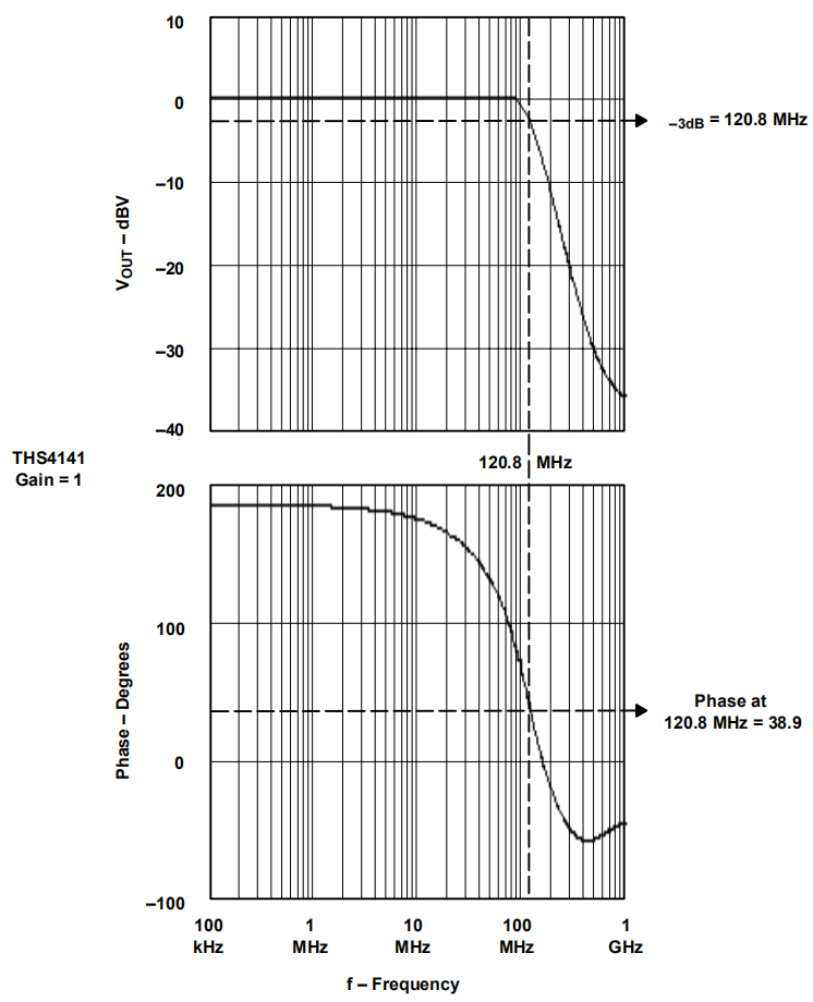
Figure 13–12. Differential Amplifier Closed-Loop Response
Figure 13–13 shows a design example of an ac-coupled, single-ended analog input drive circuit. This circuit uses a THS3201 current-feedback op amp and operates up to 975 MHz. The amplifier is configured as a noninverting amplifier with a gain of 2, where gain is 1 + R4/R3. In a current-feedback amplifier, the feedback resistor sets the amplifier bandwidth and the frequency response shape as well as defining the gain of the circuit. R4 and R3 cannot be arbitrary values.
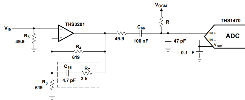
Figure 13–13. ADC Single-Ended Input Drive Circuit
The frequency response plots for a gain of 2, with R3 = R4 = 619 Ω, are shown in Figures 13–13 and 13–14. R4 affects the amplifier bandwidth and frequency response peaking. R3 has no effect on bandwidth and frequency peaking; it only affects the gain. The –3-dB bandwidth is 520 MHz. Increasing the resistance of R4 decreases the bandwidth. Conversely, lowering R4 resistance increases the bandwidth at the expense of increased peaking in the ac response.
The phase plot in Figure 13–14 exhibits a fairly linear phase shift (a flat group delay response) and hence the amplifier output should show excellent signal reproduction. Unlike a voltage-feedback amplifier, the power supply voltage affects the bandwidth of a current-feedback amplifier. For example, lowering the supply voltage of the THS3201 from ± 5 V to ± 2.5 V reduces the bandwidth from 925 MHz to 350 MHz.

Figure 13–14. Gain vs Frequency Plot for THS3201
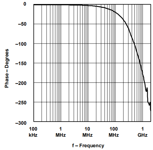
Figure 13–15. Phase vs Frequency for THS3201
No comments:
Post a Comment