Search

Designing Low-Voltage Op Amp Circuits

Introduction to Designing Low-Voltage Op Amp Circuits

In one respect, voltage is like water: you don’t appreciate its value until your supply runs low. Low-voltage systems, defined here as a single power supply less than 5 V, teach us to appreciate voltage. We aren’t the first electronic types to learn how valuable voltage is; about 15 years ago the audio console design engineers appreciated the relationship between voltage and dynamic range. They needed more dynamic range to satisfy their customers; thus, they ran op amps at the full rated voltage, not the recommended operating voltage, so they could squeeze a few more dB of dynamic range from the op amp. 

These engineers were willing to take a considerable risk running op amps at the full rated voltage; but their customers demanded more dynamic range. The moral of this story is that dynamic range is an important parameter, and supply voltage is tied directly to dynamic range. Knowing how to obtain and use the maximum dynamic range and input/output voltage range is critical to achieving success in low voltage design. We will investigate these subjects in detail later, but for now it is useful to review the history of op amps. Knowing how op amps evolved into the today’s marvels is interesting, and it gives designers an insight into system problems that they encounter as they design in the low voltage world.

When power supplies were ±15 V, the output voltage swing of an op amp didn’t seem important. When the power supply was 30 V the typical circuit designer could afford to sacrifice 3 V from each end of the output voltage swing (this was because of transistor saturation or cutoff). The transistors in the op amp need enough voltage across them to operate correctly, so why worry about 6 V out of 30 V. Also, the input transistors required base bias, so an op amp with 30-V supplies often offered a common-mode input voltage range of 24 V or less. These numbers come from the µA741 data sheet; the µA741 (about 1969) is the first internally compensated op amp to achieve wide popularity. 

A later generation op amp, the LM324, had better dynamic range characteristics than the µA741. The LM324’s output voltage swing is 26 V when operated from a 30-V power supply, and the common-mode input voltage range is 28.5 V. The LM324 was big news because it was specified to operate with a 5-V power supply. The LM324’s output voltage swing at VCC = 5 V is 3.48 V, and this presented problems for the early low voltage circuit designers because the output voltage swing was smaller than most analog-to-digital converter (ADC) input voltage ranges. You must fill the ADC input voltage range to obtain its full dynamic range. The LM324 had an input voltage common-mode range of (VCC–1.5 V) to 0 V; at least this op amp could work with transducers connected to the lower power supply rail if the transducer did not have an ac output voltage swing. 

The next incremental improvement in op amps was the LM10 because it operated on 1.1-V power supplies. It was introduced almost as an afterthought because there was no pressing demand for it. Its brilliant designer, Robert J. Widlar, wrote “IC op amps have reached a certain maturity in that there no longer seems to be a pressing demand for better performance.” There were no pressing demands for a low voltage op amp in 1978 because portable (portable means battery applications that are almost always single supply) did not become popular until the late 1980s or early 1990s.

Cell phones, calculators, and portable instruments — not new battery technology — opened the market for low-voltage op amps, and when the portable concept caught on, the demand for low-voltage op amps increased. The increasing demand did not breed new companies committed to low-voltage IC design; rather, the established IC manufacturers threw a few low voltage op amps into their portfolio. These op amps, like the LM324, could operate on a low voltage, but they were severely lacking in input common-mode voltage range and output voltage swing. Circuit designers had to be satisfied with this generation of op amps until something better came along. Well, something better is here now! 

The next generation of low-voltage op amps has much better specifications. The TLV278X operates off a power supply ranging from 1.8 V to 3.6 V, and it has an output voltage swing of 1.63 V (when the power supply is 1.8 V) coupled with an input common mode voltage range of –0.2 V to 2 V. The TLV240X operates off a power supply ranging from 2.5 V to 16 V, and it has an output voltage swing of 2.53 V when the power supply voltage is 2.7 V. Also, when it is operated off a 2.7-V power supply, it has an input common mode voltage range of –0.1 V to 7.7 V. These new op amps are far superior to their predecessors when evaluated on the their merits, which are extended output voltage swing and input common voltage range.

The latest op amps make it possible to design more accurate and cost effective electronic equipment, but there is one problem that they don’t solve. Low-voltage applications are defined here as single-supply applications, and in single-supply design, the op amp input voltage and output voltage is referenced to the midpoint of the power supply (VCC/2). Unfortunately, most transducers are not connected to the midpoint of the power supply because, in the majority of cases, this requires a third wire beyond VCC and ground. It doesn’t help to create VCC/2 at the transducer location (to save a wire) because it is not identical to the midpoint of the power supply (unresolved errors enter because of the reference voltage difference). When the transducer in a single supply design is referenced to any voltage other than the midpoint of the power supply, the reference voltage is amplified with the transducer voltage.

The trick to designing single supply op amp circuits is using external biasing to strip off or null out the reference voltage. Designing op amp circuits with biasing normally involves an iterative cut and try approach where the designer assumes a circuit configuration, solves equations, changes the configuration, and repeats the process until a solution is found. A technique that solves the problem the first time is presented later.


Dynamic Range

It is extremely hard to define dynamic range (DR) for an op amp, so lets start with a digital to-analog converter (DAC) where DR is defined as the ratio of the maximum output voltage to the smallest output voltage the DAC can produce (least significant bit or LSB). Dynamic range is usually expressed in dB using the formula given in Equation 18–1.

The same definition of DR can be used for an op amp, and the maximum output voltage swing equals VOUTMAX. This output voltage swing is defined as the maximum output voltage the op amp can achieve (VOH) minus the minimum output voltage the op amp can achieve (VOL). VOH and VOL are easily obtainable from an op amp IC data sheet. Normally, VOH and VOL are guaranteed minimum and maximum parameters respectively. This yields Equation 18–2.

Equation 18–2 can be used to illustrate the role that power supply voltage plays in limiting the DR. VOH(MIN) is the most positive power supply voltage minus the voltage drop across the upper output transistor, thus VOH(MIN) is directly proportional to the most positive power supply voltage. For any op amp, the output voltage swing is directly proportional to the power supply voltage, thus, in the same op amp, the DR is directly proportional to the power supply voltage.

At first thought, one might think that the smallest output voltage that an op amp can have is zero, and the natural conclusion based on this assumption is that the DR is equal to infinity. This is never the case because op amp and external circuit imperfections ensure that the smallest op amp output voltage is greater than zero. It turns out that VOUT(MIN) is actually determined by a series of error terms. These error terms are the op amp’s internal noise (Vn and In), external resistor noise (VnR), power supply rejection ratio (kSVR), voltage offset (VIO), current offset (IIO), common-mode rejection ratio (CMRR), and closed loop gain (G). Each of these error terms is referred to the input of the op amp, so they must be multiplied by the closed loop gain to be referred to the output (see Figure 18–1).

Figure 18–1. Op Amp Error Sources

The error sources are taken into account in Equation 18–3, and this equation refers them to the op amp output by multiplying them by the op amp’s closed loop gain.


The maximum DR that can be achieved by an op amp is given in Equation 18–4.

The DR is reduced by the sum of the error terms, so it is proper to conclude that the maximum power supply voltage and the op amp choice (this defines the error magnitude) both establish the DR of an op amp. The first two terms in Equation 18–3 are dc error terms, thus, they can be adjusted to zero by one of several methods not mentioned here. The input offset current and input bias current error terms were big factors with older generation ICs, but today’s technology render them much less significant (see Table 18–1).

Table 18–1. Comparison of Op Amp Error Terms
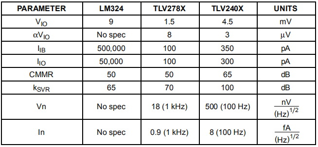
The data in Table 18–1 indicates that older low voltage op amps are not capable of yielding the DR that that later technology op amps are.


Signal-to-Noise Ratio

Noise sets a limit on the information and signals that can be handled by a system. The ability of an amplifier, receiver, or other device to discern a signal is degraded by noise. Noise mixed with the incoming signal, noise generated by the op amp, resistor noise, and power supply noise ultimately determine the size of the signal that can be recovered and measured.

Noise fluctuates randomly over a period of time, so instantaneous signal or noise levels don’t describe the situation adequately. Averages over a long period of time (root mean squared or RMS) are used to describe both the signal and the noise. Signal-to-noise ratio (SNR) was initially established as a measure of the quality of the signal that exists in the presence of noise. This SNR was a power ratio, and it was established at the output of a circuit. The SNR that we are interested in is a voltage ratio because the impedance is constant, and it is established at the input to the op amp. This means that all noise voltages, including resistor noise voltage, must be calculated in RMS volts at the op amp input. The SNR is given in Equation 18–5.

The signal is established by a transducer; a device that senses a change in a variable and converts that change into a voltage change. Transducers also convert some of their physical surroundings into a noise voltage that is combined with the signal. Noise from the physical surroundings of the transducer, unless its nature is well known, is almost impossible to separate from the transducer signal. When transducers are connected to the electronics, cabling picks up noise, and some transducers like thermocouples can pick up noise from the connecting junctions. Thus, the signal is never clean as it enters the electronics. The noise generated by the op amp was defined in the previous section as Vn, InREQ, InRR, and ∆V/kSVR, and this noise is added to the signal. The transducer often has a very small output voltage swing, so when the transducer output voltage swing is converted to least significant bits (LSB) the noise voltage should be very small compared to an LSB. Consider a temperature transducer that has a 10-mV 

swing over its range. When the transducer output voltage swing is considered to be the full-scale voltage (FSV) of an ADC, the LSB is very small as is shown in Equation 18–6 for a 12-bit (N) ADC.

The op amp for this application must be a very low noise op amp because an op amp with a 20-nV/(Hz)1/2 equivalent input noise voltage and a bandwidth of 4 MHz contributes 40 µV of noise. This high noise contribution is why extensive filtering and “optimally” low bandwidth is found desirable in the input stages of some electronic systems. If there is power supply noise, some of that noise passes through the op amp to its input. The power supply noise is divided by the power supply rejection ratio, but there is always a residual noise component of the power supply on the op amp input as shown in Equation 18–7 where kSVR is 60 dB.


Input Common-Mode Range

Years ago the op amp’s input common-mode voltage range (VICR) did not include the power supply rails. The best VICR that was available was (VCC +|VEE|–6 V), and when the input voltage approached VICR, distortion occurred. If the input voltage exceeded the power supply rails, the output stage might invert phase (it sometimes latched in the inverted position causing control problems) or the IC might self destruct. The vast majority of transducers were connected to ground (0 V) because it was easy to make a ground connection and because a split supply op amp has inputs referenced to ground. In a split supply application with the transducer connected to ground, latch-up or self destruction is unlikely. 

In special cases, transducers are connected to a power supply rail (usually VCC when power supply current sensing) or some other voltage, and in this special case, additional bias circuitry was added to split power supply designs to keep the input voltage swing within VICR. Bias circuitry in conjunction with external components removed the effects of the power supply rail connection.

Many low voltage op amp input signals come from transducers connected to a power supply rail like the circuit shown in Figure 18–2.
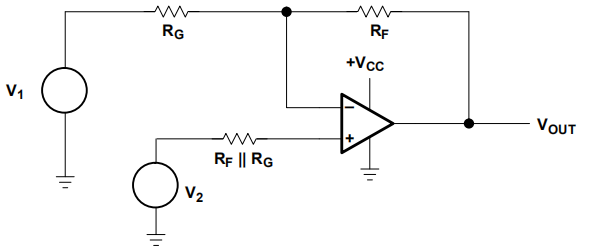

Figure 18–2. Noninverting Op Amp

When V1 = 0 and V2 is the transducer input, the op amp must be capable of handling input voltages that go to 0 V. Furthermore, the transducer voltage may be ac, so it swings above and below ground, thus the transducer voltage drops below the low power supply rail. This situation requires that the op amp’s VICR exceed the power supply voltage. Rail-to-rail input (RRI) voltage capability is a necessary requirement for a low-voltage op amp that handles transducers connected to a power supply rail. 

When the input voltage is connected to ground and the input voltage swing is very small, a standard op amp like the LM324 suffices. Referring to Figure 18–3 it can be seen that the PNP input transistors are biased by the emitter current source. If the positive input is connected to ground bias current still flows and the transistor stays active. If the input transistors are selected very carefully for operation with low collector-base junction reverse bias, the input voltage can go slightly below ground (–200 mV for the TLV278X) and the op amp will still operate correctly. The circuit operation is one sided though because when the input voltage approaches the positive supply rail, the emitter current source and input transistors turn off. This type of circuit does not offer rail-to-rail operation, but it does offer from rail to (VCC –1.5V) operation.
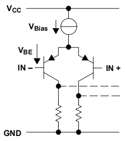

Figure 18–3. Input Circuit of a NonRRI Op Amp

An op amp with a NPN input stage works in a similar way around the positive supply rail. It can sense voltages close to VCC and maybe slightly above VCC, but it won’t work when it is within 1.5 V of ground. The solution for this problem is to include parallel input circuits as shown in Figure 18–4.
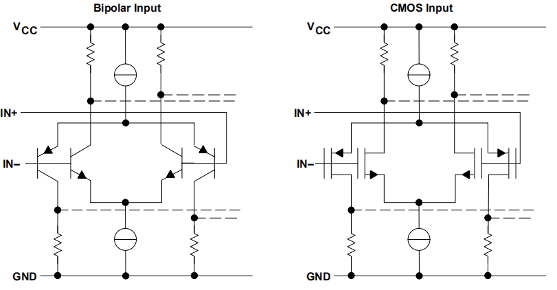
Figure 18–4. Input Circuit of an RRI Op Amp

The RRI op amps have parallel input stages. There are both PNP and NPN differential amplifiers used in the input stages of the RRI op amp, thus the RRI op amp can operate above and below the power supply voltage. As Figure 18–4 shows, the parallel input stages can be made in bipolar or MOS technology.

The input stages operate in three different ranges. When the input voltage ranges from about –0.2 V to 1 V, the PNP differential amplifier is active and the NPN differential amplifier is cutoff. When the input voltage ranges from about 1 V to (VCC –1 V), both the NPN and PNP differential amplifiers are active. When the input voltage ranges from about (VCC –1 V) to (VCC + 0.2 V), the NPN differential amplifier is active and the PNP differential amplifier is cut off. Inclusion of complementary differential input amplifiers achieves VICR exceeding the power supply limits, but there is a penalty to pay in input bias current, input offset voltage, and distortion. Figures 18–5 and 18–6 show the input bias current and input offset voltage as a function of the input common-mode voltage.
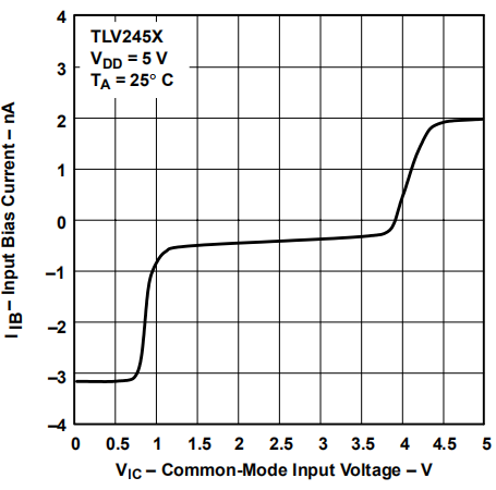
Figure 18–5. Input Bias Current Changes with Input Common-Mode Voltage

Figure 18–6. Input Offset Voltage Changes with Input Common-Mode Voltage

When both transistors are conducting current the input bias currents have a tendency to cancel, so in the range of ±1 V, the bias current is extremely low even when bipolar transistors are used to make the op amp. Above this range, the PNP differential amplifier cuts off so the full bias current requirement of the NPN transistor becomes apparent. The same action happens below this range when the NPN differential amplifier cuts off. Notice that the PNP bias current is significantly larger than the NPN bias current; this is expected because NPN transistors have better gain characteristics than PNP transistors. The base emitter voltage of the NPN and PNP transistors is well matched because the magnitude of the input offset voltage at the extremes is almost equal. The bias current and offset voltage variation with input signal amplitude cause errors and distortion of the input signal. Inserting a resistance equal to the parallel combination of RF and RG into the positive op amp lead minimizes the effect of input bias current. The resistor, RP, has the same voltage drop across it that the parallel combination of RF and RG has, hence the bias current is converted to a common-mode voltage. The common mode voltage is normally in the µV-range because IIB is in the fractional nA range and RP is in the tens of KΩ. The CMMR is approximately 60 dB, so the input bias current effect is reduced to the nV range where it is insignificant compared to the offset voltage. The input offset current is multiplied by RP, and it shows up as an input error. If the design can’t tolerate these errors it is wise to switch to a CMOS op amp because its input currents are in the pA range.

Another type of error creeps in when complementary differential amplifiers are used to obtain DR, and this error is results from the different gain of the PNP and NPN transistors.

Op amps always suffer to a limited extent from distortion introduced by different gains when operating in different quadrants The positive quadrant is above VCC/2 where NPN transistors operate, and the negative quadrant is below VCC/2 where the PNP transistors operate. Normally, this is a very minor effect because only the gain of the output stage changes with quadrant, but with complementary input stages the input and output gains change with quadrant. These errors are small, and they are accepted as the sacrifice required for obtaining RRI operation.


Output Voltage Swing

Rail-to-rail output voltage swing (RRO) is desirable for at least two reasons. First, the DR can achieve the maximum obtainable value if the op amp is RRO. Second RRO op amps can drive any converter connected to the same power supply if the impedance is compatible. The schematic of a RRO op amp output stage, part of the TLC227X, is shown in Figure 18–7.

Figure 18–7. RRO Output Stage

The RRO characteristic is achieved in the construction of the op amp output stage. A totem pole design that has upper and lower output transistors is used, and the output transistors are a complimentary pair. Each transistor in the pair is a “self-locking” type of transistor operating in the common-source mode. Consider the p-channel output transistor; as long as this transistor has a drain-source resistance it forms a voltage divider with the load resistance. When the load is a very large resistor or if the output current flow is very small, the voltage drop across the output transistor can be neglected. Output current flows through the output transistor, and because current drops a voltage (VDS) across the drain source resistor, the output voltage swing is reduced. The voltage drop subtracts from the power supply voltage, reducing the output voltage to less than RRO. 

RRO op amps can’t drive heavy loads and maintain their RRO capability because of the voltage dropped across the output transistors. Load resistance or output current is a test condition when the measurement of an op amp’s output voltage swing is made. The size of the load resistor or output current is a measure of the op amp’s ability to retain its RRO capability while sourcing or sinking an output current. When selecting a RRO op amp, the designer must consider the load resistance or output current required because these conditions control the output voltage swing. 

When an op amp is made that has RRI and RRO capability, it is called a rail-to-rail input/output op amp. This long name is shortened to RRIO.


Shutdown and Low Current Drain

Low voltage design often is accompanied by a requirement that the power supply current drain be low. The power supply current drain is kept low to decrease battery size and prolong battery charge so recharging can be put off as long as possible. Many methods are employed to keep the current drain low including using high-value resistors, low bias current regulators/references, slow speed logic, keeping logic transitions to a minimum, low voltage power supplies, selecting op amps for low current drain, and shutting off unused ICs. 

High-value resistors have less current flowing through them than low value resistors do, and they can be used effectively in ratio applications, but there are some downsides to using high-value resistors. When resistor values exceed 2 MΩ to 10 MΩ, depending on the type of resistor, the temperature drift, vibration, and time-induced drift increases rapidly compared to that of lower value resistors. The input resistor to an op amp, RG, works with the stray capacitance from the input node to ground to form a pole in the loop gain. As the resistance increases, the pole moves towards the zero frequency intercept and the circuit overshoots, rings, or becomes unstable. The feedback resistor, RF, works with stray capacitance in parallel with RF to form a low-pass filter. Sometimes this filter action is desirable, but the filter often distorts the signal.

Very often, low bias current regulators and references are just standard ICs specified at a lower current. These devices generally do not have the same small tolerances at low bias currents that they had at high bias currents. Although they are more often costly, redesigned low bias current regulators and references are becoming available. Ensure that the reference or regulator bias current used in the application is the same as that used to specify the device, because sometimes the error curves for references are nonlinear. Also, investigate the reference noise voltage to ensure that low bias current has not moved the device to a noisy portion of its operating curve. Saturated logic is the choice for low current drain applications because nonsaturated logic stays in the active region and has a higher current drain. Always pick the slowest logic gates that you can get away with. Speed in saturated logic requires enough current to drive low impedance loads, and that means high power supply currents coupled with logic-generated noise. High-speed logic has a low impedance totem pole output stage, and every time the output is switched, both totem pole transistors are on causing a current spike through the power supply. Large decoupling capacitors are required to localize the current spike at the logic IC, thus preventing noise propagation. CMOS logic draws the least quiescent current, and if the logic transitions are kept at a minimum, the current drain stays small. One method of minimizing logic transitions is to use asynchronous logic. 

The op amp should be selected with current drain in mind. Three rail-to-rail op amps have widely differing current drains because they are designed for different applications. The TLV240X is designed for micropower applications, and its current drain is 1.29 µA. The TLV411X is designed high output drive, and its current drain is 800 µA. The TLV287X is designed for high speed, and its current drain is 820 µA. These three op amps are low-voltage op amps, but they each serve a different application. 

The best method of conserving current is to shut the op amp down if you are not using it. Most op amps designed for low voltage applications have shutdown pins. A typical op amp that draws 820 µA when operating, draws 1.7 µA when it is shut down. The problem with shutdown is the time that it takes to wake the op amp up and knowing when to wake the op amp up. A typical low-voltage op amp turns on in less that 1 µs, but the system designer usually has to choose the variable that eventually wakes the op amp up.


Single-Supply Circuit Design

The op amp is a linear device, so it follows the equation of a straight line. The equation of a straight line has four forms as shown in Equation 18–8.

These four forms can be implemented with four single supply circuits. When the designer discovers the form of Equation 18–8 that yields the transform function required, it is a small task to find the corresponding circuit. Once the circuit and transfer function are established, the task reduces to matching coefficients between the transfer function and the circuit equation, and then calculating the resistor values. The key required to unlock the puzzle is to determine the form of Equation 18–8 that yields the required transfer function. 

This key is found in simultaneous equations because they define the equation of a straight line. Several examples of using simultaneous equations to determine the required form of the op amp transfer function are given in the next two sections.


Transducer to ADC Analog Interface

An example is a transducer that needs to be interfaced to an ADC. The transducer specifications are VMIN = 0.2 V, VMAX = 0.5 V, and ROUT = 600 Ω. The ADC specifications are VIN(LOW) = 1.5 V, VIN(HIGH) = 4.5 V, and RIN = 20 kΩ. The system specifies a 5-V power supply and 5% tolerance resistors. The transducer is connected to input of the amplifier (see Figure 18–8), so its output voltage swing is renamed VIN, and the ADC is connected to the output of the amplifier, so its input voltage range is renamed VOUT. Now, two data points are constructed as VIN1 = 0.2 V @ VOUT1 = 1.5 V and VIN2 = 0.5 V @ VOUT2 = 4.5 V. 

The data points are substituted into the equation Y = mX + b; m is named the slope and b is named the X axis intercept or just the intercept for short. Don’t worry about the sign of m or b because it is determined by the math, and it is substituted into the equation that determines the transfer equation. The simultaneous equations are given below.
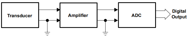
Figure 18–8. Data Acquisition System

From these equations we find that b = –0.5 and m = 10. The slope and intercept values are substituted into Equation 18–8 to get Equation 8–11.

The mathematical terminology in Equation 18–11 is replaced by electronics terminology in Equation 18–12, and this is the transfer function required for the amplifier. The next step is to select the op amp, and this isn’t a hard task because there are many candidates that could do the job with these undemanding specifications, so let us not dwell on the selection process. Assume that the selected op amp operates on a 5-V power supply, can drive the ADC input resistance of 20 kΩ with no voltage divider action, and that the op amp input impedance is so big that it doesn’t load the transducer.

The circuit that produces the desired transfer function is given in Figure 18–9.

Figure 18–9. Schematic for the Transducer to ADC Interface Circuit

The circuit equation is obtained with the aid of superposition.

Comparing terms between Equations 18–12 and 18–13 enables the extraction of m and b.
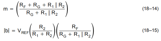
Making the assumption that R1||R2<<RG simplifies the calculations.

Let RG = 20 kΩ, and then RF = 180 kΩ, add, and let VREF = VCC.

Select R2 = 0.82 kΩ and R1 = 72.98 kΩ. Since 72.98 kΩ is not a standard 5% resistor value, R1 is selected as 75 kΩ. The difference between the selected and calculated value of R1 introduces about 3% error in the b coefficient, and this error shows up in the transfer function as an intercept rather than a slope error. The parallel resistance of R1 and R2 is approximately 0.82 kΩ and this is much less than RG which is 20 kΩ, thus the earlier assumption that R1||R2<<RG is justified. R2 could have been selected as a smaller value, but the smaller values yielded poor standard 5% values for R1. The final circuit is shown in Figure 18–10.

Figure 18–10. Final Schematic for the Transducer to ADC Interface Circuit


DAC to Actuator Analog Interface

An amplifier is also used to interface a DAC with an actuator (see Figure 18–11).

Figure 18–11. Digital Control System

The interface is different from the ADC interface because the DAC output signal is usually current rather than voltage. The first inclination is to stuff the DAC output into a current-to voltage converter like we have always done with split power supplies. This doesn’t always work because the DAC current can be sinked or sourced from ground or the power supply. If a current sourced from the positive power supply is put into a standard current-to-voltage circuit, it wants to drive the op amp output negative, and you need a negative resistor to counter this. The alternate solution for a sourced current from the positive power supply is to terminate the DAC output in a resistor that converts current into voltage, and then 

level shift and amplify the terminated voltage. The circuit that performs this function is shown in Figure 18–12.
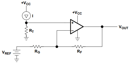
Figure 18–12. DAC Current Source to Actuator Interface Circuit

The DAC output current sources from IOUT(ZEROS) = 1 mA to IOUT(ONES) = 2 mA at an output compliance of 4.33 V. The actuator requires an input voltage swing of VIN1 = 1 V to VIN2 = 4 V to drive it, and its input resistance is 100 kΩ. The system specifications include one 5-V power supply and 5% resistors. The DAC is connected to input of the amplifier (see Figure 18–11), so its output current swing is renamed IIN, and the actuator is connected to the output of the amplifier, so its input voltage range is renamed VOUT. Now, two data points are constructed as IIN1 = 1 mA @ VOUT1 = 1 V and IIN2 = 2 mA @ VOUT2 = 4 V. The data points are substituted into the Equation 18–20. Don’t worry about the sign of m or b because it is determined by the math, and it is substituted into the equation that determines the transfer equation. The simultaneous equations are given below.

From these equations we find that b = –2 and m = 3. The slope and intercept values are substituted into Equation 18–20 to get Equation 18–23.

The equation for the circuit shown in Figure 18–12 is derived with the aid of superposition, and it is given below in Equation 18–24.

Comparing terms between Equations 18–20 and 18–24 enables the extraction of m and b.

These equations are written in terms of mA and kΩ, so RT = 2.14 kΩ. There is no 2.14-kΩ resistor in the 5% standard values; thus, RT is split into 1.8-kΩ and 0.33-kΩ resistors. RG is selected as 51 kΩ, so RF = 20 kΩ. When IIN = 2 mA VRT = 4.28 V, so the compliance of the DAC is not violated. You might find that standard DACs are not so generous with their compliance specifications. 

When the current is sinked from the power supply by the DAC its sign reverses and the previous circuit is not usable. Consider these specifications: the DAC output sinks current from the power supply IOUT(ZEROS) = –1 mA to IOUT(ONES) = –2 mA at an output compliance of 4.33 V. The actuator requires an input voltage swing of VIN1 = 1 V to VIN2 = 4 V to drive it, and its input resistance is 100 kΩ. The system specifications include one 5-V power supply and 5% resistors. The DAC is connected to input of the amplifier (see Figure 18–11), so its output current swing is renamed IIN, and the actuator is connected to the output of the amplifier, so its input voltage range is renamed VOUT. Now, two data points are constructed as IIN1 = –1 mA @ VOUT1 = 1 V and IIN2 = –2 mA @ VOUT2 = 4 V. The data points are substituted into the Equation 18–20. Don’t worry about the sign of m or b because it is determined by the math, and it is substituted into the equation that determines the transfer equation. The transfer function for the current sink DAC is given in Equation 18–29.

The simultaneous equations are given below.
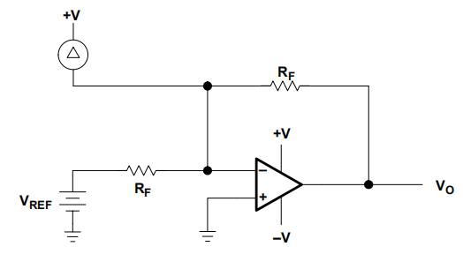
Figure 18–13. DAC Current Sink to Actuator Interface Circuit

From these equations we find that b = –2 and m = –3. The slope and intercept values are substituted into Equation 18–28 to get Equation 18–32.

The current equation for the circuit shown in Figure 18–13 is given below as Equation 18–33, and after algebraic manipulation it becomes Equation 18–34.
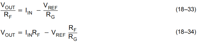
Comparing terms between Equations 18–29 and 18–34 enables the extraction of m and b.

These equations are written in terms of mA and kΩ. RG is selected as 51 kΩ, so RF = 20 kΩ. When IIN = 2 mA, the compliance of the DAC is 0.0 V.

When DAC interface circuits are designed, two parameters that have not been considered in detail can control the design. The DAC has a compliance voltage requirement, and that requirement must be met regardless of the circuit demands. If the DAC compliance requirements are not met, the DAC saturates or is starved for current, and either of these situations introduces considerable error. The actuators driven in these examples are quite benign because most actuators require considerably more current or voltage than is available from an op amp. This fact does not negate the analysis given here. Regardless of the actuator current or voltage requirements, the design procedure is similar. Very often the low voltage device is plugged into a booster that supplies power to the actuator. 

One last item to consider is the output capacitance of DACs. The DAC output can have large amounts of stray capacitance that shows up as a capacitor across the op amp inverting input node when the DAC is interfaced into circuits as shown in Figure 18–13. The DAC capacitance from the inverting node to ground acts with RG to form a pole in the op amp loop gain. Adding a pole to the op amp loop gain leads to overshoot, then ringing, and finally oscillation. The effect that the DAC capacitance has on stability must be investigated. Also, the DAC output capacitance is a function of the digital number addressing the DAC. This capacitance can range from near zero to hundreds of pF, thus the op amp must be compensated for the worst case which is the largest capacitance.

Compensation schemes include connecting a capacitor across the feedback resistor. This compensation scheme is called a compensated attenuator, and if the RC time constants are equal, there will excellent performance at that DAC output capacitance.  Alas, the circuit can only be ideally compensated at one point, and this point is normally chosen as the highest DAC output capacitance. The remainder of the DAC range suffers from poor bandwidth because of overcompensation.


Comparison of Op Amps

Since the author is only familiar with Texas Instruments op amps, a comparison involving actual op amp parameters would be unfair to other op amp manufacturers. Also, any comparison using today’s production op amps becomes invalid in a short period of time. I write about Texas Instruments op amps, so I get plenty of samples, and the new product introductions come so fast that I have a hard time keeping up with them. The other point to consider is that teaching how to make the op amp comparison is a much more powerful tool, thus a table containing the op amp parameters is established, and each of the parameters is discussed only in terms of low-voltage design.

Table 18–2. Op Amp Parameters

Table 18–2. Op Amp Parameters.png

As the table shows, there are a lot of parameters to be considered in the selection of a low voltage op amp. The application weeds out some of these parameters thus easing the selection process. If the application is measuring the output from a low-bandwidth transducer such as a thermocouple, bandwidth is not a parameter of interest, so speed can immediately be sacrificed for power supply current. 

When the maximum supply voltage available is 3 V, rafts of op amps requiring more than 3 V operating voltage are eliminated. Taking this concept further, if dynamic range is an important specification in the 3-V design, those op amps that operate on 3 V without RRIO specifications can be eliminated. Because dynamic range is important, the noise voltage and current that detract from dynamic range are important parameters. If this 3-V application requires very low power supply current, the choice is narrowed down to a few candidates. The application selects the op amp, and if this application puts a few more requirements on the 3-V op amp, we may have to design a new IC.

Always start the selection process with the parameter that absolutely can’t be wavered. The next parameter considered in the selection process should be the next most important parameter, and this process is continued parameter by parameter until all requirements are exhausted. Sometimes the supply of op amp candidates runs out before the parameter requirements do. When you reach this point, it is time to renegotiate the design specifications, find a new op amp, negotiate with op amp manufacturers, or announce that you won’t meet specifications. These designs are hard to work because the low power supply voltage requirement and the specifications usually leave very little room to work. As time marches on, more low power supply voltage op amps will come on the market, and these designs will get easier to work.

Circuit Board Layout Techniques

The PCB is a Component of the Op Amp Design

Op amp circuitry is analog circuitry, and is very different from digital circuitry. It must be partitioned in its own section of the board, using special layout techniques. Printed circuit board effects become most apparent in high-speed analog circuits, but common mistakes described in this chapter can even affect the performance of audio circuits. The purpose of this chapter is to discuss some of the more common mistakes made by designers and how they degrade performance, and provide simple fixes to avoid the problems. 

In all but very rare cases, the PCB layout for analog circuitry must be designed such that the effect of the PCB is transparent to the circuit. Any effect caused by the PCB itself should be minimized, so that the operation of the analog circuitry in production will be the same as the performance of the design and prototype.


Prototype

Normal design cycles, particularly of large digital boards, dictate layout of the PCB as soon as possible. The digital circuitry has been simulated, but in most cases, the production PCB itself is the prototype, and may even be sold to a customer. Digital designers can correct small mistakes by implementing cuts and jumpers, reprogramming gate arrays or flash memories, and go on to the next project. This is not the case with analog circuitry. 

Some of the common design mistakes discussed in this chapter cannot be corrected by the cut and jumper method. They can and will render the entire PCB unusable. It is very important for the digital designer, who is used to cuts and jumpers, to read and understand this chapter prior to releasing a board to a layout service. A little care, taken up front, can save a board worth thousands of dollars from becoming scrap because of blunders in a tiny section of analog circuitry. This author has been the unfortunate recipient of a simple analog circuit designed by another engineer, who was accustomed to the cut and jumper method of correcting his mistakes. This resulted in a design that was full of mistakes. Not only was the op amp hooked up with inverting and noninverting inputs reversed, but an RC time constant had to be added to prevent a race condition. Repercussions from these mistakes, and associated rework problems, caused literally hundreds of hours to be lost from a tight production schedule. Prototyping this circuit would have taken less than a day. PROTOTYPE ALL ANALOG CIRCUITRY!


Noise Sources

Noise is the primary limitation on analog circuitry performance. Internal op amp noise is covered in Chapter 10. Other types of noise include: 

  • Conducted Emissions — noise that the analog circuitry generates through its connections to other circuits. This is usually negligible in analog circuitry, unless it is high power (such as an audio amplifier that draws heavy currents from its power supply). 

  • Radiated Emissions — noise that the analog circuitry generates, or transmits, through the air. This is also usually negligible in analog circuitry, unless it is high frequency such as video. 

  • Conducted Susceptibility — noise from external circuitry that is conducted into the analog circuit through its connections to other circuits. Analog circuitry must be connected to the “outside world” by at least a ground connection, a power connection, an input, and an output. Noise can be conducted into the circuit through all of these paths, as well as any others that are present. 

  • Radiated Susceptibility — noise that is received through the air (or transmitted into the analog circuitry) from external sources. Analog circuitry, in many cases, resides on a PCB that may have high-speed digital logic including DSP chips. High-speed clocks and switching digital signals create considerable radio frequency interference (RFI). Other sources of radiated noise are endless: the switching power supply in a digital system, cellular telephones, broadcast radio and TV, fluorescent lighting, nearby PCs, lightning in thunderstorms, and so on. Even if the analog circuitry is primarily audio in frequency, RFI may produce noticeable noise in the output.


PCB Mechanical Construction

It is important to choose a PCB with the right mechanical characteristics for the application.

1. Materials — Choosing the Right One for the Application

PC Board materials are available in various grades, as defined by the National Electrical Manufacturers Association (NEMA). It would be very convenient for designers if this organization was closely allied with the electronics industry — controlling parameters such as resistivity and dielectric constant of the material. Unfortunately, that is not the case. NEMA is an electrical safety organization, and the different PCB grades primarily describe the flammability, high temperature stability, and moisture absorption of the board. Therefore, specifying a given NEMA grade does not guarantee electrical parameters of the material. If this becomes critical for an application, consult the manufacturer of the raw board stock. Laminated materials are designated with FR (flame resistant) and G grades. FR–1 is the least flame resistant, and FR–5 is the most. G10 and G11 have special characteristics as described in Table 17–1.

Table 17–1. PCB Materials


Do not use FR–1. There are many examples of boards with burned spots, where high wattage components have heated a section of the board for a period of time. This grade of PCB material has more in common with cardboard than anything else. 

FR–4 is commonly used in industrial-quality equipment, while FR–2 is used in high-volume consumer applications. These two board materials appear to be industry standards. Deviating from these standards can limit the number of raw board material suppliers and PCB houses that can fabricate the board because their tooling is already set up for these materials. Nevertheless, there are applications in which one of the other grades may make sense. For very high frequency applications, it may even be necessary to consider Teflon or even ceramic board substrate. One thing can be counted on, however: the more exotic the board substrate, the more expensive it will be. In selecting a board material, pay careful attention to the moisture absorption. Just about every desirable performance characteristic of the board will be negatively impacted by moisture. This includes surface resistance of the board, dielectric leakage, high-voltage breakdown and arcing, and mechanical stability. Also, pay attention to the operating temperature. High operating temperatures can occur in unexpected places, such as in proximity to large digital ICs that are switching at high speeds. Be aware that heat rises, so if one of those 500-pin monster ICs is located directly under a sensitive analog circuit, both the PCB and circuit characteristics may vary with the temperature. 

After the board substrate material has been selected, the next decision is how thick to make the copper foil laminated to it. For most applications, 1-ounce copper is sufficient. If the circuit consumes a lot of power, 2-ounce may be better. Avoid -ounce copper, because it tends to break between the trace and the pad.

2. How Many Layers are Best?

Depending on the complexity of the overall circuitry being designed, a designer must decide how many layers the PCB should be.

2.1. Single-Sided

Very simple consumer electronics are sometimes fabricated on single-sided PCBs, keeping the raw board material inexpensive (FR–1 or FR–2) with thin copper cladding. These designs frequently include many jumper wires, simulating the circuit routing on a double sided board. This technique is only recommended for low-frequency circuitry. For reasons described below, this type of design is extremely susceptible to radiated noise. It is harder to design a board of this type, because of the many things can go wrong. Many complex designs have been successfully implemented with this technique, but they require a lot of forethought. An example is a television set that puts all of the analog circuitry on a single-sided board at the bottom of the case, and uses the metallized CRT itself to shield the board from a separate digital tuning board near the top of the set. Be prepared to get creative if the design demands high volume, low cost PCBs. If a single-sided PCB is a requirement, remember the trace resistance! The op amp is not a 3-terminal device (inverting input, noninverting input, and output). It is a 7-terminal device as shown in Figure 17–1.

Figure 17–1. Op Amp Terminal Model

Resistance in the power leads of the device must be taken into account, as well as resistance between the return for the inputs and the load. Both the input and load must return somewhere. If these are at different potentials due to trace resistance, there can be problems.

2.2. Double-Sided

The next level of complexity is double-sided. Although there are some double-sided FR–2 boards, they are more commonly fabricated with FR–4 material. The increased strength of FR–4 material supports vias better. Doubled-sided boards are easier to route because there are two layers of foil, and it is possible to route signals by crossing traces on different layers. Crossing traces, however, is not recommended for analog circuitry. Wherever possible, the bottom layer should be devoted to a ground plane, and all other signals routed on the top layer. A ground plane provides several benefits: 

  • Ground is frequently the most common connection in the circuit. Having it continuous on the bottom layer usually makes the most sense for circuit routing. 

  • It increases mechanical strength of the board. 

  • It lowers the impedance of all ground connections in the circuit, which reduces undesirable conducted noise. 

  • It adds a distributed capacitance to every net in the circuit — helping to suppress radiated noise. 

  • It acts a shield to radiated noise coming from underneath the board.

2.3. Multi-Layer

Double-sided boards, in spite of their benefits, are not the best method of construction, especially for sensitive or high-speed designs. The most common board thickness is 1.5 mm. This separation is too great for full realization of some of the benefits listed above. Distributed capacitance, for example, is very low due to the separation. 

Critical designs call for multi-layer boards. Some of the reasons are obvious: 

  • Better routing for power as well as ground connections. If the power is also on a plane, it is available to all points in the circuit simply by adding vias. 

  • Other layers are available for signal routing, making routing easier. 

  • There will be distributed capacitance between the power and ground planes, reducing high frequency noise. 

There are other reasons for multi-layer boards, however, that may not be obvious or intuitive.

  • Better EMI/RFI rejection. There is due to the image plane effect, which has been known since the time of Marconi. When a conductor is placed close to a parallel conductive surface, most of the high frequency currents will return directly under the conductor, flowing in the opposite direction. This mirror image of the conductor within the plane creates a transmission line. Since currents are equal and opposite in the transmission line, it is relatively immune to radiated noise. It also couples the signal very efficiently. The image plane effect works equally well with ground and power planes, but they must be continuous. Any gap or discontinuity causes the beneficial effects to quickly vanish. There is more on this in the following paragraphs. 

  • Reduced overall project cost for small production runs. Although multi-layer boards are more expensive to manufacture, EMI/RFI requirements from the FCC or other agencies may require expensive testing of the design. If there are problems, it can force a complete redesign of the PCB, leading to additional rounds of testing. A multi-layer PCB can have as much as 20-dB better EMI/RFI performance over a 2-layer PCB. If production volumes are going to be small, it makes sense to make a better PCB to begin with, than try to cut costs and take the risk of failing $25,000 to $50,000 tests.


3. Board Stack-Up — The Order of Layers

There has been a lot of confusion in the past over what is the optimum order for PCB layers. Take, for example, a 4-layer board consisting of two signal layers, a power plane, and a ground plane. Is it better to route the signal traces between the layers, thus providing shielding for the signal traces – or is it better to make the ground and power planes the two inner planes? 

In considering this question, it is important to remember that no matter what is decided, there will still be signals exposed on one or both of the top and bottom planes. The leads of the op amp PCB package, and the traces on the board leading to nearby passive components and feed throughs will be exposed. Therefore, any shielding effects are compromised. It is far better to take advantage of the distributed capacitance between the power and ground plane by making them internal. 

Another advantage of placing the planes internally is that the signal traces are available for probing and modification on the top and bottom layers. Anyone who has had to change connections on buried traces will appreciate this feature. For more than four layers, it is a general rule to shield higher speed signals between the ground and power planes, and route slower signals on the outer layers.


Grounding

Good grounding is a system-level design consideration. It should be planned into the product from the first conceptual design reviews.

1. The Most Important Rule: Keep Grounds Separate

Separate grounding for analog and digital portions of circuitry is one of the simplest and most effective methods of noise suppression. One or more layers on multi-layer PCBs are usually devoted to ground planes. If the designer is not careful, the analog circuitry will be connected directly to these ground planes. The analog circuitry return, after all, is the same net in the netlist as digital return. Autorouters respond accordingly and connect all of the grounds together, creating a disaster. 

After the fact separation of grounds on a mixed digital and analog board is almost impossible. Every ground connection in the analog circuitry must be lifted from the board and connected together. For surface mount boards, this results in a colossal mess of “tombstoned” passive components and floating IC leads.

2. Other Ground Rules

  • Ground and power planes are at the same ac potential, due to decoupling capacitors and distributed capacitance. Therefore, it is important to isolate the power planes as well. 

  • Do not overlap digital and analog planes (Figure 17–2). Place analog power coincident with analog ground, and digital power coincident with digital ground. If any portion of analog and digital planes overlap, the distributed capacitance between the overlapping portions will couple high-speed digital noise into the analog circuitry. This defeats the purpose of isolated planes.

Figure 17–2. Digital and Analog Plane Placement

  • Separate grounds does not mean that the grounds are electrically separate in the system. They have to be common at some point, preferably a single, low-impedance point. System-wise, there is only one ground, and it is the electrical safety ground in an ac-powered system or battery ground in a dc-powered system. Everything else “returns” to that ground. It would be a good idea to develop the discipline to refer to everything that is not a ground as a return. All returns should be connected together at a single point, which is system ground. At some point, this will be the chassis. It is important to avoid ground loops by multiple connections to the chassis. Ensuring only one chassis ground point is one of the most difficult aspects of system design.


Figure 17–3. Separate Grounds

  • If at all possible, dedicate separate connector pins to separate returns, and combine the returns only at system ground. Aging and repeated mating causes connector pins to increase in contact resistance, so several pins are needed. Many digital boards consist of many layers and hundreds or thousands of nets. The addition of one more net is seldom an issue, but the addition of several connector pins almost always is. If this cannot be done, then it will be necessary to make the two returns a single net on the PCB — with very special routing precautions. 

  • It is important to keep digital signals away from analog portions of the circuit. It makes little sense to isolate planes, keep analog traces short, and place passive components carefully if there are high-speed digital traces running right next to the sensitive analog traces. Digital signals must be routed around analog circuitry, and not overlap analog ground and power planes. If not, the design will include a new schematic symbol shown in Figure 17–4 — the broadcasting antenna! 

Most digital clocks are high enough in frequency that even small capacitances between traces and planes can couple significant noise. Remember that it is not only the fundamental frequency of the clock that can cause a potential problem, but also the higher frequency harmonics.


Figure 17–4. Broadcasting From PCB Traces

  • It is a good idea to locate analog circuitry as close as possible to the I/O connections of the board. Digital designers, used to high current ICs, will be tempted to make a 50-mil trace run several inches to the analog circuitry thinking that reducing the resistance in the trace will help get rid of noise. What they have actually done is create a long, skinny capacitor that couples noise from digital ground and power planes into the op amp, making the problem worse!

3. A Good Example

Figure 17–5 shows one possible board layout. In this system, all electronics, including the power supply, reside on one PCB. Three separate and isolated ground/power planes are employed: one for power, one for digital, and one for analog. Power and ground connections from digital and analog sections of the board are combined only in the supply section, and are combined in close proximity. High-frequency conducted noise on the power lines is limited by inductors (chokes). In this case, the designer has even located low frequency analog circuitry close to low speed digital, keeping high frequency digital and analog physically apart on the board. This is a good, careful design that has a high likelihood of success — providing that good layout and decoupling rules are also followed.


Figure 17–5. A Careful Board Layout

4. A Notable Exception

There is one case where it is necessary to combine analog and digital signals on the analog ground plane. Analog to digital (A/D) and digital to analog (D/A) converters are packaged as ICs with analog and digital ground pins coming out of the package. One might assume, based on the previous discussion, that the digital ground pin should be connected to digital ground and the analog ground pin to analog ground. That, however, is not correct. 

The pin names analog ground and digital ground refer to internal connections in the IC, not the plane to which they should be connected. Both should connect to the analog ground plane. The connection would have been made inside the IC, but it is impossible to get low enough impedance at the typical geometries inside ICs. The IC designer actually counts on the end user to supply a low impedance connection outside the IC. Otherwise, the performance of the converter will be worse than specified.

One might suspect that the digital portions of the converter would make circuit performance worse by coupling digital switching noise onto the analog ground and power plane. Converter designers realize this, and design digital portions without a lot of output power to minimize switching transients. If the converter does not drive large fanouts, this should not be a problem. Be sure to properly decouple the logic supply for the converter to analog ground (see the following paragraphs).


The Frequency Characteristics of Passive Components

Choosing the right passive components for an analog design is important. In most cases, a right passive component will fit on the same pads as a wrong passive component, but not always. Start the design process by carefully considering the high frequency characteristics of passive components, and putting the correct part outline on the board from the start. 

Most designers are totally ignorant of the frequency limitations of the passive components they use in analog circuitry. Passive components have limited frequency ranges, and operation of the part outside of that range can have some very unexpected results. One might think that this discussion only applies to high-speed analog circuits. But high frequencies that are radiated or conducted into a low-speed circuit will affect passive components as well. For example: a simple op amp low-pass filter may well turn into a high-pass filter at RF frequencies.

1. Resistors

High-frequency performance of resistors is approximated by the schematic shown in Figure 17–6.

Figure 17–6. Resistor High-Frequency Performance

Resistors are typically one of three types: wire-wound, carbon composition, and film. It does not take a lot of imagination to understand how wire-wound resistors can become inductive because they are coils of resistive wire. Most designers are not aware of the internal construction of film resistors, which are also coils of thin metallic film. Therefore, film resistors are also inductive at high frequencies. The inductance of film resistors is lower, however, and values under 2 kΩ are usually suitable for high frequency work. 

The end caps of resistors are parallel, and there will be an associated capacitance. Usually, the resistance will make the parasitic capacitor so “leaky” that the capacitance does not matter. For very high resistances, the capacitance will appear in parallel with the resistance, lowering its impedance at high frequencies.

2. Capacitors

High-frequency performance of capacitors is approximated by the schematic shown in FIgure 17–7.

Figure 17–7. Capacitor High-Frequency Performance

Capacitors are used in analog circuitry for power supply decoupling and as filter components. For an ideal capacitor, reactance decreases by the formula:

Therefore, a 10-µF electrolytic capacitor has a reactance of 1.6 Ω at 10 kHz, and 160-µΩ at 100 MHz. Right?

In reality, one will never see the 160 µΩ with the electrolytic capacitor. Film and electrolytic capacitors have layers of material wound around each other, which creates a parasitic inductance. Self-inductance effects of ceramic capacitors are much smaller, giving them a higher operating frequency. There is also some leakage current from plate to plate, which appears as a resistance in parallel with the capacitor, as well as resistance within the plates themselves, which add a parasitic series resistance. The electrolyte itself in electrolytic capacitors is not perfectly conductive (to reduce leakage current). These resistances combine to create the equivalent series resistance (ESR). The capacitors used for decoupling should be low ESR types, as any series resistance limits the effectiveness of the capacitor for ripple and noise rejection. Elevated temperatures also severely increase ESR, and can be permanently destructive to capacitors. Therefore, if an aluminum electrolytic will be subjected to high temperatures, use the high-temperature grade (1050C), not the low temperature grade (850C).

For leaded parts, the leads themselves also add a parasitic inductance. For small values of capacitance, it is important to keep the lead lengths short. The combination of parasitic inductance and capacitance can produce resonant circuits! Assuming a lead self-inductance of 8 nH/cm (see the following paragraphs), a 0.01-µF capacitor with two 1-cm leads will resonate at 12.5 MHz. This effect was well known to engineers many decades ago, who designed vacuum tube-based products with leaded components. Woe be to any hobbyist restoring antique radios that is unaware of this effect! 

If electrolytic capacitors are used in a design, make sure that the polarity is correctly observed. The positive terminal of the capacitor must be connected to the more positive of two dc potentials. If there is any doubt whatsoever which polarity is correct, design calculations must continue until it is known, or a prototype must be built. Incorrect polarity of electrolytic capacitors will cause them to conduct dc current, in most cases destroying the part — and probably the rest of the circuit as well. If there is a rare case in which there will be both polarities present, use a nonpolarized electrolytic (which is constructed by connecting two polarized electrolytic capacitors in series). Of course, one can always connect two capacitors in series on the PCB, keeping in mind that the effective capacitance will be cut in half for equal values of capacitor.

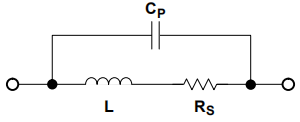
3. Inductors

High frequency performance of inductors is approximated by the schematic shown in Figure 17–8.

Figure 17–8. Inductor High-Frequency Performance

Inductive reactance is described by the formula:

Therefore, a 10-mH inductor has a reactance of 628 Ω at 10 kHz, which increases to 6.28 MΩ at 100 MHz. Right? 

In reality, one will never see the 6.28 MΩ with this inductor. Parasitic resistances are easy to understand — the inductor is constructed of wire, which has a given resistance per unit length. Parasitic capacitance is harder to visualize, unless one considers the fact that each turn of wire in the inductor is located next to adjacent turns, forming a capacitor. This parasitic capacitance limits the upper frequency of this inductor to under 1 MHz. Even small wire-wound inductors start to become ineffective in the 10 MHz to 100 MHz range.

4. Unexpected PCB Passive Components

In addition to the obvious passive components above, the PCB itself has characteristics that form components every bit as real as those discussed previously — just not as obvious.

4.1. PCB Trace Characteristics

The layout pattern on a PCB can make it susceptible to radiated noise. A good layout is one that minimizes the susceptibility of analog circuitry to as many radiated noise sources as possible. Unfortunately, there is always a level of RF energy that will be able to upset the normal operation of the circuit. If good design techniques are followed, that level will be one that the circuit never encounters in normal operation.

4.1.1. Trace Antennas

A board is susceptible because the pattern of traces and component leads form antennas. Antenna theory is a complex subject, well beyond the scope of this book. Nevertheless, a few basics are presented here. One basic type of antenna is the whip, or straight conductor. This antenna works because a straight conductor has parasitic inductance, and therefore can concentrate flux from external sources. The impedance of any straight conductor has a resistive and an inductive component:

For dc and low frequencies, resistance is the major factor. As the frequency increases, however, the inductance becomes more important. Somewhere in the range of 1 kHz to 10 kHz, the inductive reactance exceeds the resistance, so the conductor is no longer a low resistance connection, but rather an inductor. 

The formula for the inductance of a PCB trace is:

The inductance is relatively unaffected by the diameter, since it varies as the logarithm of the circumference. Common wires and PCB traces vary between 6 nH and 12 nH per centimeter. 

For example, a 10 cm PCB trace has a resistance of 57 mΩ and an inductance of 8 nH per cm. At 100 kHz, the inductive reactance reaches 50 mΩ. At frequencies above 100 kHz, the trace is inductive — not resistive.

A rule of thumb for whip antennas is that they begin to couple significant energy at about 1/20 of the wavelength of the received signal, peaking at  the wavelength. Therefore, the 10-cm conductor of the previous paragraph will begin to be a fairly good antenna at frequencies above 150 MHz. Remember that although the clock generator on a digital PCB may not be operating at a frequency as high as 150 MHz, it approximates a square wave. Square waves will have harmonics throughout the frequency range where PCB conductors become efficient antennas. If through-hole components are mounted in a way that leaves significant lead length, those component leads also become antennas, particularly if they are bent. 

Another major type of antenna is the loop. The inductance of a straight conductor is dramatically increased by bending it into partial or complete loops. Increased inductance lowers the frequency at which the conductor couples radiated signals into the circuit.

Without realizing it, most digital designers are well versed in loop antenna theory. They know not to make loops in critical signal pathways. Some designers, however, that would never think of making a loop with a high speed clock or reset signal will turn right around and create a loop by the technique they use for layout of the analog section of the board. Loop antennas constructed as loops of wire are easy to visualize. What is not as obvious is that slot antennas are just as efficient. Consider the three cases shown in Figure 17–9.

Figure 17–9. Loop and Slot Antenna Board Trace Layouts

Version A is a poor design. It does not use an analog ground plane at all. A loop is formed by the ground and signal traces. An electric field E and perpendicular magnetic field H are created, and form the basis of a loop antenna. A rule of thumb for loop antennas is that the length of each leg is equal to half the most efficiently received wavelength. Remember, however, that even at 1/20 of the wavelength, the loop will still be a fairly efficient antenna.

Version B is a better design, but there is intrusion into the ground plane, presumably to make room for a signal trace. A much smaller slot antenna is formed by the difference in pathways between signal and return. A second loop is created by the cutout for the IC. 

Version C is the best design. Signal and return are coincident with each other, eliminating loop antenna effects completely. Note that there is still a cutout for the IC, but it is located away from the return path for the signal.

4.1.2. Trace Reflections

Reflections and matching are closely related to loop antenna theory, but different enough to warrant their own discussion. 

When a PCB trace turns a corner at a 900 angle, a reflection can occur. This is primarily due to the change of width of the trace. At the apex of the turn, the trace width is increased to 1.414 times its width. This upsets the transmission line characteristics, especially the distributed capacitance and self–inductance of the trace — resulting in the reflection. It is a given that not all PCB traces can be straight, and so they will have to turn corners. 

Most CAD systems give some rounding effect on the trace. Sharp 900 corners in traces are a relic of the tape up days of PCB layout. The rounding effects of CAD programs, however, still do not necessarily maintain constant width as the trace rounds the corner. Figure 17–10 shows progressively better techniques of rounding corners. Only the last example maintains constant trace width and minimizes reflections. Most CAD programs now support these methods, but they can entail a little more work to master.

Figure 17–10. PCB Trace Corners

A suggestion for the advanced PCB layout engineer: leave rounding to the last step before tear-dropping and flood-filling. Otherwise, the CAD program will slow down doing numerical calculations as the traces are moved around during routing.

4.2. Trace-to-Plane Capacitors

PCB traces, being composed of foil, form capacitance with other traces that they cross on other layers. For two traces crossing each other on adjacent planes, this is seldom a problem. Coincident traces (those that occupy the same routing on different layers), form a long, skinny capacitor. The formula for capacitance is shown in Figure 17–11.

Figure 17–11. PCB Trace-to-Plane Capacitance Formula

For example, if the capacitance formula is applied to the following trace: 

  • 4 Layer board — signal routing next to ground plane 

  • Board layer thickness: 0.188 mm 

  • Trace Width: 0.75 mm 

  • Trace Length: 7.5 mm 

A typical value for ER of FR–4 PCB material is 4.5. Due to the variations of material from which an FR–4 board can be fabricated, this value is not guaranteed, but should be in the range of 4 to 5.

The capacitance between these traces would be 1.1 pF. Of course, the antenna effect on a 7.5-mm trace would be devastating, so this example is a bit extreme. Ignoring the antenna effects for now, there are cases in which even a very small parasitic capacitance like 1 pF is unacceptable. Figure 17–12 dramatically illustrates the effect of 1 pF capacitance occurring at the inverting input of the op amp. It causes a doubling of the output amplitude near the bandwidth limit of the op amp. This is an invitation to oscillation, especially since the trace is an efficient antenna above 180 MHz.

Figure 17–12. Effect of 1-pF Capacitance on Op Amp Inverting Input

There are numerous fixes to the problem above. The most obvious would be to shorten the length of the traces. Another not-so-obvious fix would be to use a different trace width. There is no reason why an inverting op amp trace has to be 0.75 mm wide — it carries almost no current. If the trace length is reduced to 2.5 mm (one third as long) and the trace width is changed to 0.188 mm (1/4 as wide), the capacitance becomes 0.1 pF — much less significant in the example above. Another fix is to remove the ground plane under the inverting input and the traces leading to it. 

The inverting input of op amps, particularly high-speed op amps, is especially prone to oscillation in high gain circuits. This is due to unwanted capacitance on the input stage. It is important to minimize capacitance on this input by reducing trace width and placing components as close as possible to this input. If this input still oscillates, it may be necessary to scale the input and feedback resistors lower by a decade or two to change the resonance of the circuit. Scaling the resistors up will seldom help, as the problem is also related to the impedance of the circuit. If filter components are involved, they will also have to be scaled to avoid changing the filter characteristics of the circuit. The power consumption of the circuit will also increase if resistors are lowered.

4.3. Trace-to-Trace Capacitors and Inductors

PCB traces are not infinitely thin. They have some finite thickness, as defined by the ounce parameter of the copper clad foil. The higher the number of ounces, the thicker the copper. If two traces run side-by-side, then there will be capacitive and inductive coupling between them (Figure 17–13). The formulas for these parasitic effects can be found in transmission line and/or microstrip references, but are too complex for inclusion here.

Figure 17–13. Coupling Between Parallel Signal Traces

Signal lines should not be routed parallel to each other, unless transmission line or microstrip effects are desired. Otherwise, a gap of at least three times the signal trace width should be maintained. 

Capacitance between traces in an analog design can become a problem if fixed resistors in the design are large (several MΩ). Capacitance between the inverting and noninverting inputs of an op amp could easily cause oscillation.

4.4. Inductive Vias

Whenever routing constraints force a via (connection between layers of a PCB, FIgure 17–14), a parasitic inductor is also formed. At a given diameter (d) the approximate inductance (L) of an via at a height of (h) may be calculated as follows:

Figure 17–14. Via Inductance Measurements

For example, a 0.4-mm diameter via through a 1.5-mm thick PCB has an inductance of 1.1 nH. 

Keep in mind that inductive vias combined with parasitic capacitance can form resonant circuits. The self-inductance of a via is small enough that these resonances are in the GHz range, but inductors add in series, lowering the resonant frequency. Do not put several vias on a critical trace of a high-speed analog circuit! Another concern is that the vias put holes in ground planes, potentially creating ground loops. They should be avoided — the best analog layout is one that routes all signal traces on the top layer of the PCB.

4.5. Flux Residue Resistance

Yes, even an unclean board can affect analog circuit performance. 

Be aware that if the circuit has very high resistances — even in the low MΩ — special attention may need to be paid to cleaning. A finished assembly may be adversely affected by flux or cleansing residue. The electronics industry in the past few years has joined the rest of the world in becoming environmentally responsible. Hazardous chemicals are being removed from the manufacturing process — including flux that has to be cleaned with organic solvents. Water-soluble fluxes are becoming more common, but water itself can become contaminated easily with impurities. These impurities will lower the insulation characteristics of the PCB substrate. It is vitally important to clean with freshly distilled water every time a high-impedance circuit is cleaned. There are applications that may call for the older organic fluxes and solvents, such as very low power battery powered equipment with resistors in the 10s of MΩ range. Nothing can beat a good vapor defluxing machine for ensuring that the board is clean.


Decoupling

Noise, of course, can propagate into analog circuitry through the power pins of the circuit as a whole and op amp itself. Bypass capacitors are used to reduce the coupled noise by providing low impedance power sources local to the analog circuitry.

1. Digital Circuitry — A Major Problem for Analog Circuitry

If analog circuitry is located on the same board with digital circuitry, it is important to understand a little about the electrical characteristics of digital gates. 

A typical digital output consists of two transistors connected in series between power and ground (Figure 17–15). One transistor is turned on and the other turned off to produce logic high and vice versa for logic low. Because one transistor is turned off for either logic state, the power consumption for either logic state is low, while the gate is static at that level.

Figure 17–15. Logic Gate Output Structure

The situation changes dramatically whenever the output switches from one logic state to the other. There may be a brief period of time when both transistors conduct simultaneously. During this period of time, current drawn from the power supply increases dramatically — since there is now a low impedance path through the two transistors from power to ground. Power consumption rises dramatically and then falls, creating a droop on the power supply voltage, and a corresponding current spike. The current spike will radiate radio frequency (RF) energy. There may be dozens, or even hundreds of such outputs on a digital IC, so the aggregate effect may be quite dramatic. 

It is impossible to predict the frequencies of these spikes, because the frequencies are affected by the propagation delays of the transistors in the gate. Propagation delay is affected by random factors that occur during manufacture. Digital switching noise will be broadband, with harmonics throughout the spectrum. A general rejection technique is required, rather than one that rejects a specific frequency.

2. Choosing the Right Capacitor

Table 17–2 is a rough guideline describing the maximum useful frequencies of common capacitor types.

Table 17–2. Recommended Maximum Frequencies for Capacitors

Obviously from the table, tantalum electrolytic capacitors are useless for frequencies above 1 MHz. Effective high frequency decoupling at higher frequencies demands a ceramic capacitor. Self-resonances of the capacitor must be known and avoided or the capacitor may not help, or even make the problem worse. Figure 17–16 illustrates the typical self-resonance of two capacitors commonly used for bypassing — 10 µF tantalum electrolytic and 0.01 µF ceramic.

Figure 17–16. Capacitor Self Resonance

Consider these resonances to be typical values, the characteristics of actual capacitors can vary from manufacturer to manufacturer and grade of part to grade of part. The important thing is to make sure that the self-resonance of the capacitor occurs at a frequency above the range of the noise that must be rejected. Otherwise, the capacitor will enter a region where it is inductive. 

Do not assume that a single 0.1-µF capacitor will decouple all frequencies. Smaller capacitors may work better at higher frequencies than larger ones. When poor decoupling at higher frequencies is suspected, try a smaller capacitor rather than a larger one.

3. Decoupling at the IC Level

The method most often used to decouple the high-frequency noise is to include a capacitor, or multiple capacitors connected from the op amp power pin to the op amp ground pin. It is important to keep the traces on this decoupling capacitor short. If not, the traces on the PCB will have significant self-inductance, defeating the purpose of the capacitor.

A decoupling capacitor must be included on every op amp package — whether it contains 1, 2 or 4 devices per package. The value of capacitor must be picked carefully to reject the type of noise present in the circuit. In particularly troublesome cases, it may be necessary to add a series inductor into the power supply line connecting to the op amp. This inductor is in addition to the decoupling capacitors, which are the first line of defense. The inductor should be located before, not after the capacitors. 

Another technique that is lower in cost is to replace the series inductor with a small resistor in the 10-Ω to 100-Ω range. The resistor forms a low-pass filter with the decoupling capacitors. There is a penalty to pay for this technique — depending on the power consumption of the op amp, it will reduce the rail-to-rail voltage range. The resistor forms a voltage divider with the op amp as a resistive active component in the lower leg of the divider. Depending on the application, this may or may not be acceptable.

4. Decoupling at the Board Level

There is usually enough low frequency ripple on the power supply at the board input to warrant a bulk decoupling capacitor at the power input. This capacitor is used primarily to reject low frequency signals, so an aluminum or tantalum capacitor is acceptable. An additional ceramic cap at the power input will decouple any stray high frequency switching noise that may be coupled off of the other boards.


Input and Output Isolation

Many noise problems are the result of noise being conducted into the circuit through its input and output pins. Due to the high-frequency limitations of passive components, the response of the circuit to high frequency noise may be quite unpredictable. 

In situations in which conducted noise is substantially different in frequency from the normal operating range of the circuit, the solution may be as simple as a passive RC low-pass filter that rejects RF frequencies while having negligible effect at audio frequencies. A good example is RF noise being conducted into an audio op amp circuit. Be careful, though. A low pass filter loses its characteristics at 100 to 1000 times f3db. More stages may be required to cover different frequency ranges. If this is the case, make the highest frequency filter the one nearest to the source of noise. Inductors or ferrite beads can also be used in a noise rejection filter network to eliminate conducted noise. Ferrite beads are inductive up to a specified frequency, and then become resistive.

The effect of radiated energy coupling into an analog circuit can be so bad that the only solution to the problem may be to completely shield the circuit from radiated energy. This shield is called a Faraday Cage, and must be carefully designed so that frequencies that are causing the problem are not allowed to enter the circuit. This means that the shield must have no holes or slots larger that 1/20 the wavelength of the offending frequency. This can be a demanding requirement. It is a good idea to design a PCB from the beginning to have enough room to add a metal shield if it becomes necessary. If a shield is used, frequently the problem will be severe enough that ferrite beads will also be required on all connections to the circuit.


Packages

Op amps are commonly supplied one, two, or four per package. Single op amps often contain additional inputs for features such as offset nulling. Op amps supplied two and four per package only offer inverting and noninverting inputs, and the output. If the additional features are important, the only package choice is single. Be aware, though, that the offset-nulling pins on a single op amp package can act as secondary inputs, and must be treated carefully. Consult the data sheet on the particular device being used.

Figure 17–17. Common Op Amp Pinouts

The single op amp package places the output on the opposite side from the inputs. This can be a disadvantage at high speeds, because it forces longer PCB traces. One way to overcome this difficulty is to use a surface-mount package, and mount the feedback components on the rear of the board. This, however, adds at least two vias to the design, and places a hole in the ground plane for a 2-layer design. It may make more sense to use a dual op amp package, even if the second op amp is unused (remember to terminate it properly — see paragraph 17.7.3). Figure 17–18 is an illustration of trace length for an inverting op amp stage.


Figure 17–18. Trace Length for an Inverting Op Amp Stage

It is popular to use dual op amps for stereophonic circuits, and quad op amps for filter stages with many sections. There is a penalty for doing so, however. Although modern processing techniques provide high levels of isolation between amplifiers on the same piece of silicon, there will be some crosstalk. If isolation between amplifiers is important, then single packages should be considered. Crosstalk problems are not limited to the IC – the dual and quad packages place a high density of passive components in close proximity to each other. This proximity will lead to some crosstalk. 

Dual and quad op amp packages offer some additional benefits beyond density. The amplifier stages tend to be mirror images of each other. If similar stages are to be laid out on the PCB, the layout only needs to be done once, then it can be mirror-imaged to form the other stage. Figure 17–19 illustrates this effect for four inverting op amp stages implemented in a quad package:

Figure 17–19. Mirror-Image Layout for Quad Op Amp Package

These illustrations, however, do not show all connections required for operation, in particular, the half-supply generator for single-supply operation. Modifying the diagram of Figure 17–19 to use the fourth op amp as a half supply generator is shown in Figure 17–20.

Figure 17–20. Quad Op Amp Package Layout with Half-Supply Generator

This example shows all of the connections actually required to produce three independent inverting stages. Note that the half-supply connection can be made entirely under the IC, keeping the trace length short. This example is not meant to be used as a suggested PCB layout, it merely illustrates what can be done. The half-supply op amp, for example, could be any one of the four. The passive components can be selected so that they span the lead pitch. Surface-mount 0402 packages, for example, span a width equal to or less than a standard SO package. This can keep traces lengths extremely short for high frequency applications. 

Package styles for op amps include the dual-in-line (DIP) and small-outline (SO). Lead pitches for op amps have been continually decreasing, as has been the case for all ICs in general. Decreasing lead pitches have been accompanied by a decrease in the size of passive components as well. Decreasing the overall circuit dimensions reduces parasitic inductance, which should allow higher frequency circuits, but it also increases the potential for crosstalk by placing conductors closer to each other where capacitive effects increase.


1. Through-Hole Considerations

The older technology for op amps and other components is through-hole. Components are constructed with leads that insert through holes in the board — hence the name. Through-hole components, due to their size, are more suited to applications where space is not an issue. The components themselves are frequently lower in cost, but the PCB is more expensive due to the fact that the PCB fabrication house has to drill holes for component leads. PCBs are primarily a mechanical fabrication — the number of holes and number of different drills have a big impact on the price. 

The leads on a through-hole op amp are arranged on a 0.1-inch grid. Many PCB layout people like to maintain the 0.1-inch grid for the rest of the components as well. Resistors and other passive components can even be purchased with leads pre-bent to land on a 0.1 inch grid. Some electrolytic capacitors have leads that are on a 0.025-inch grid. These component sizes may force a lot of wasted area on the PCB. Components that ideally should be placed close to the op amp itself may be forced several tenths of an inch away, due to intervening components. Therefore, through hole circuitry is not recommended for high speed analog circuitry, or for analog circuitry in proximity to high speed digital. 

Some designers attempt to overcome the long trace length caused by resistors by placing the resistors on the board vertically, one lead of the resistor bent close to the body of the part. This is common in older consumer electronics. This allows for denser placement of parts, and may help some with trace length — but each resistor exposes almost 1 cm of one component lead to radiated signals, and lead self-inductance.

An advantage of the through-hole approach of PCB layout is that the through-holes themselves can serve as feed throughs, reducing the number of vias in complex circuits.

2. Surface Mount

Surface-mount circuitry does not require a hole for each component lead. Automated testing, however, may require vias on every node. The holes were never an issue with through-hole circuitry, because every component lead made a hole in the board. The PCB layout designer, who is used to designing a board with a minimum number of vias, now has to put a via on EVERY node of the circuit. This can make a Swiss cheese out of a nice continuous ground plane — negating many of the advantages it provides. 

Fortunately, there is a close variation of the “via on every node” requirement. This requirement can often be met by putting a test pad on every node. The automated test station can then access the analog circuitry from the top of the board. A clamshell test fixture is significantly more expensive than one that accesses only one side of the board. The extra cost can be justified if there is documentation that circuit performance will be unacceptable with vias. 

Signal connections to ground or the power supply may have to be made through a small fixed resistor instead, so the automated equipment can access that pin of the IC and test its function.

3. Unused Sections

In many op amp designs, one or more op amps may be unused. If this is the case, the unused section must be terminated properly. Improper termination can result in greater power consumption, more heat, and more noise in op amps on the same physical IC. If the unused section of the op amp is connected as shown in the better side of Figure 17–21, it will be easier to use it for design changes.

Figure 17–21. Proper Termination of Unused Op Amp Sections


Summary

1. General :

  • Think of the PCB as a component of the design. 

  • Know and understand the types of noise the circuit will be subjected to. 

  • Prototype the circuit.


2. Board Structure :

  • Use a high-quality board material such as FR–4. 

  • Multi-layer boards are as much as 20-dB better than double-sided boards. 

  • Use separate, non overlapping ground and power planes. 

  • Place power and ground planes to the interior of the board instead of exterior.

3. Components :

  • Be aware of frequency limitations of traces and other passive components. 

  • Avoid vertical mounting of through-hole passive components in high-speed circuits. 

  • Use surface mount for high-speed analog circuitry. 

  • Keep traces as short as possible. 

  • Use narrow traces if long traces are required. 

  • Terminate unused op amp sections properly.

4. Routing :

  • Keep analog circuitry close to the power connector of the board. 

  • Never route digital traces through analog sections of the board, or vice versa. 

  • Make sure that traces to the inverting input of the op amp are short. 

  • Make sure that traces to the inverting and noninverting inputs of the op amp do not parallel each other for any significant length. 

  • It is better to avoid vias, but the self-inductance of vias is small enough that a few should cause few problems. 

  • Do not use right angle traces, use curves if at all possible.

5. Bypass

  • Use the correct type of capacitor to reject the conducted frequency range. 

  • Use tantalum capacitors at power input connectors for filtering power supply ripple. 

  • Use ceramic capacitors at power input connectors for high frequency conducted noise. 

  • Use ceramic capacitors at the power connections of every op amp IC package. More than one capacitor may be necessary to cover different frequency ranges. 

  • Change the capacitor to a smaller value — not larger — if oscillation occurs. 

  • Add series inductors or resistors for stubborn cases. 

  • Bypass analog power only to analog return, never to digital return.

Main History About Op Amp