Introduction to Voltage- and Current-Feedback Op Amp Comparison
The name, operational amplifier, was given to voltage-feedback amplifiers (VFA) when they were the only op amps in existence. These new (they were new in the late ’40s) amplifiers could be programmed with external components to perform various math operations on a signal; thus, they were nicknamed op amps. Current-feedback amplifiers (CFA) have been around approximately twenty years, but their popularity has only increased in the last several years. Two factors limiting the popularity of CFAs is their application difficulty and lack of precision.
The VFA is familiar component, and there are several variations of internally compensated VFAs that can be used with little applications work. Because of its long history, the VFA comes in many varieties and packages, so there are VFAs applicable to almost any job. VFA bandwidth is limited, so it can’t function as well at high signal frequencies as the CFA can. For now, the signal frequency and precision separates the applications of the two op amp configurations.
The VFA has some other redeeming virtues, such as excellent precision, that makes it the desirable amplifier in low frequency applications. Many functions other than signal amplification are accomplished at low frequencies, and functions like level-shifting a signal require precision. Fortunately, precision is not required in most high frequency applications where amplification or filtering of a signal is predominant, so CFAs are suitable to high frequency applications. The lack of precision coupled with the application difficulties prevents the CFA from replacing the VFA.
Precision
The long-tailed pair input structure gives the VFA its precision; the long-tailed pair is shown in Figure 9–1

Figure 9–1. Long-Tailed Pair
The transistors, Q1 and Q2, are very carefully matched for initial and drift tolerances. Careful attention is paid to detail in the transistor design to insure that parameters like current gain, β, and base-emitter voltage, VBE, are matched between the input transistors, Q1 and Q2. When VB1 = VB2, the current, I, splits equally between the transistors, and VO1 = VO2.
As long as the transistor parameters are matched, the collector currents stay equal. The slightest change of VB1 with respect to VB2 causes a mismatch in the collector currents and a differential output voltage |VB1–VB2|. When temperature or other outside influences change transistor parameters like current gain or base-emitter voltage, as long as the change is equal, it causes no change in the differential output voltage. IC designers go to great lengths to ensure that transistor parameter changes due to external influences do not cause a differential output voltage change. Now, the slightest change in either base voltage causes a differential output voltage change, and gross changes in external conditions do not cause a differential output voltage change. This is the formula for a precision amplifier because it can amplify small input changes while ignoring changes in the parameters or ambient conditions.
This is a simplified explanation, and there are many different techniques used to ensure transistor matching. Some of the techniques used to match input transistors are parameter trimming, special layout techniques, thermal balancing, and symmetrical layouts. The long-tailed pair is an excellent circuit configuration for obtaining precision in the input circuit, but the output circuit has one fault. The output circuit collector impedance has to be high to achieve high gain in the first stage. High impedance coupled with the Miller capacitance discussed in Chapter 7 forms a quasidominant pole compensation circuit that has poor high frequency response.
The noninverting input of the CFA (see Figure 9–2) connects to a buffer input inside the op amp. The inverting input of the CFA connects to a buffer output inside the CFA. Buffer inputs and outputs have dramatically different impedance levels, so any matching becomes a moot point. The buffer can’t reject common-mode voltages introduced by parameter drifts because it has no common-mode rejection capability. The input current causes a voltage drop across the input buffer’s output impedance, RB, and there is no way that this voltage drop can be distinguished from an input signal.

Figure 9–2. Ideal CFA
The CFA circuit configuration was selected for high frequency amplification because it has current-controlled gain and a current-dominant input. Being a current device, the CFA does not have the Miller-effect problem that the VFA has. The input structure of the CFA sacrifices precision for bandwidth, but CFAs achieve usable bandwidths ten times the usable VFA bandwidth.
Bandwidth
The bandwidth of a circuit is defined by high frequency errors. When the gain falls off at high frequencies unequal frequency amplification causes the signal to become distorted. The signal loses its high frequency components; an example of high frequency signal degradation is a square wave with sharp corners that is amplified and turned into slump cornered semi sine wave. The error equation for any feedback circuit is repeated in Equation 9–1.

This equation is valid for any feedback circuit, so it applies equally to a VFA or a CFA. The loop gain equation for any VFA is repeated as Equation 9–2.

Equation 9–2 is rewritten below as Equations 9–3 and 9–4 for the noninverting and inverting circuits respectively. In each case, the symbol GCLNI and GCLI represent the closed loop gain for the noninverting and inverting circuits respectively.
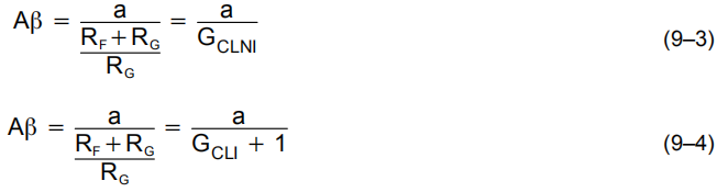
In both cases the loop gain decreases as the closed loop gain increases, thus all VFA errors increase as the closed loop gain increases. The error increase is mathematically coupled to the closed loop gain equation, so there is no working around this fact. For the VFA, effective bandwidth decreases as the closed loop gain increases because the loop gain decreases as the closed loop gain increases.
A plot of the VFA loop gain, closed loop gain, and error is given in Figure 9–3. Referring to Figure 9–3, the direct gain, A, is the op amp open loop gain, a, for a noninverting op amp. The direct gain for an inverting op amp is (a(ZF/(ZG + ZF))). The Miller effect causes the direct gain to fall off at high frequencies, thus error increases as frequency increases because the effective loop gain decreases. At a given frequency, the error also increases when the closed loop gain is increased.

Figure 9–3. VFA Gain versus Frequency
The CFA is a current operated device; hence, it not nearly as subject to the Miller effect resulting from stray capacitance as the VFA is. The absence of the Miller effect enables the CFA’s frequency response to hold up far better than the VFA’s does. A plot of the CFA loop gain, transimpedance, and error is given in Figure 9–4. Notice that the transimpedance stays at the large low frequency intercept value until much higher frequencies than the VFA does.

Figure 9–4. CFA Gain vs Frequency
The loop gain equation for the CFA is repeated here as Equation 9–5.

When the input buffer output resistance approaches zero, Equation 9–5 reduces to Equation 9–6.

Equation 9–6 shows that the closed-loop gain has no effect on the loop gain when RB = 0, so under ideal conditions one would expect the transimpedance to fall off with a zero slope. Figure 9–4 shows that there is a finite slope, but much less than that of a VFA, and the slope is caused by RB not being equal to zero. For example, RB is usually 50 Ω when RF = 1000 Ω at ACL = 1. If we let RF = RG, then RF||RG = 500 Ω, and RB/RF||RG = 50/500 = 0.1.
Substituting this value into Equation 9–6 yields Equation 9–7, and Equation 9–7 is almost identical to Equation 9–6. RB does cause some interaction between the loop gain and the transimpedance, but because the interaction is secondary the CFA gain falls off with a faster slope.

The direct gain of a VFA starts falling off early, often at 10 Hz or 100 Hz, but the transimpedance of a CFA does not start falling off until much higher frequencies. The VFA is constrained by the gain-bandwidth limitation imposed by the closed loop gain being incorporated within the loop gain. The CFA, with the exception of the effects of RB, does not have this constraint. This adds up to the CFA being the superior high frequency amplifier.
Stability
Stability in a feedback system is defined by the loop gain, and no other factor, including the inputs or type of inputs, affects stability. The loop gain for a VFA is given in Equation 9–2. Examining Equation 9–2 we see that the stability of a VFA is depends on two items; the op amp transfer function, a, and the gain setting components, ZF/ZG.
The op amp contains many poles, and if it is not internally compensated, it requires external compensation. The op amp always has at least one dominant pole, and the most phase margin that an op amp has is 45°. Phase margins beyond 60° are a waste of op amp bandwidth. When poles and zeros are contained in ZF and ZG, they can compensate for the op amp phase shift or add to its instability. In any case, the gain setting components always affect stability. When the closed-loop gain is high, the loop gain is low, and low loop gain circuits are more stable than high loop gain circuits.
Wiring the op amp to a printed circuit board always introduces components formed from stray capacitance and inductance. Stray inductance becomes dominant at very high frequencies, hence, in VFAs, it does not interfere with stability as much as it does with signal handling properties. Stray capacitance causes stability to increase or decrease depending on its location. Stray capacitance from the input or output lead to ground induces instability, while the same stray capacitance in parallel with the feedback resistor increases stability.
The loop gain for a CFA with no input buffer output impedance, RB, is given in Equation 9–6. Examining Equation 9–6 we see that the stability of a CFA depends on two items: the op amp transfer function, Z, and the gain setting component, ZF. The op amp contains many poles, thus they require external compensation. Fortunately, the external compensation for a CFA is done with ZF. The factory applications engineer does extensive testing to determine the optimum value of RF for a given gain. This value should be used in all applications at that gain, but increased stability and less peaking can be obtained by increasing RF. Essentially this is sacrificing bandwidth for lower frequency performance, but in applications not requiring the full bandwidth, it is a wise tradeoff.
The CFA stability is not constrained by the closed-loop gain, thus a stable operating point can be found for any gain, and the CFA is not limited by the gain-bandwidth constraint. If the optimum feedback resistor value is not given for a specific gain, one must test to find the optimum feedback resistor value.
Stray capacitance from any node to ground adversely affects the CFA performance. Stray capacitance of just a couple of pico Farads from any node to ground causes 3 dB or more of peaking in the frequency response. Stray capacitance across the CFA feedback resistor, quite unlike that across the VFA feedback resistor, always causes some form of instability. CFAs are applied at very high frequencies, so the printed circuit board inductance associated with the trace length and pins adds another variable to the stability equation.
Inductance cancels out capacitance at some frequency, but this usually seems to happen in an adverse manner. The wiring of VFAs is critical, but the wiring of CFAs is a science. Stay with the layout recommended by the manufacturer whenever possible.
Impedance
The input impedance of a VFA and CFA differ dramatically because their circuit configurations are very different. The VFA input circuit is a long-tailed pair, and this configuration gives the advantages that both input impedances match. Also, the input signal looks into an emitter-follower circuit that has high input impedance. The emitter-follower input impedance is β(re + RE) where RE is a discrete emitter resistor. At low input currents, RE is very high and the input impedance is very high. If a higher input impedance is required, the op amp uses a Darlington circuit that has an input impedance of β2(re + RE).
So far, the implicit assumption is that the VFA is made with a bipolar semiconductor process. Applications requiring very high input impedances often use a FET process. Both BIFET and CMOS processes offer very high input impedance in any long-tailed pair configuration. It is easy to get matched and high input impedances at the amplifier inputs. Do not confuse the matched input impedance at the op amp leads with the overall circuit input impedance. The input impedance looking into the inverting input is RG, and the impedance looking into the noninverting input is the input impedance of the op amp. While these are two different impedances, they are mismatched because of the circuit not the op amp.
The CFA has a radically different input structure that causes it to have mismatched input impedances. The noninverting input lead of the CFA is the input of a buffer that has very high input impedance. The inverting input lead is the output of a buffer that has very low impedance. There is no possibility that these two input impedances can be matched.
Again, because of the circuit, the inverting circuit input impedance is RG. Once the circuit gain is fixed, the only way to increase RG is to increase RF. But, RF is determined by a tradeoff between stability and bandwidth. The circuit gain and bandwidth requirements fix RF, hence there is no room to further adjust RF to raise the resistance of RG. If the manufacturer’s data sheet says that RF = 100 Ω when the closed-loop gain is two, then RG = 100 Ω or 50 Ω depending on the circuit configuration. This sets the circuit input impedance at 100 Ω. This analysis is not entirely accurate because RB adds to the input impedance, but this addition is very small and dependent on IC parameters. CFA op amp circuits are usually limited to noninverting voltage applications, but they serve very well in inverting applications that are current-driven.
The CFA is limited to the bipolar process because that process offers the highest speed. The option of changing process to BIFET or CMOS to gain increased input impedance is not attractive today. Although this seems like a limiting factor, it is not because CFAs are often used in low impedance where the inputs are terminated in 50 Ω or 75 Ω. Also, most very high-speed applications require low impedances.
Equation Comparison
The pertinent VFA and CFA equations are repeated in Table 9–1. Notice that the ideal closed-loop gain equations for the inverting and noninverting circuits are identical. The ideal equations for the VFA depend on the op amp gain, a, being very large thus making Aβ large compared to one. The CFA needs two assumptions to be valid to obtain the ideal equations. First, the ideal equations for the CFA depend on the op amp transimpedance, Z, being very large thus making Aβ large compared to one. Second, RB must be very small compared to ZF||ZG.
The ideal gain equations are identical, but the applications are very different because the VFA is best applied to lower frequency precision jobs while the CFA applications are in the very high frequency realm. The transimpedance in a CFA acts much like the gain does in a VFA. In each case, transimpedance or gain, it is the parameter that enables the use of feedback.
Table 9–1. Tabulation of Pertinent VFA and CFA Equations


No comments:
Post a Comment